Force detector and acceleration detector and method of manufacturing the same

a technology of force detector and acceleration detector, which is applied in the direction of acceleration measurement using interia forces, instruments, force/torque/work measurement, etc., can solve the problems of high manufacturing cost, high equipment cost, and high equipment cos

Inactive Publication Date: 2008-07-31
OKADA KAZUHIRO
View PDF70 Cites 11 Cited by
  • Summary
  • Abstract
  • Description
  • Claims
  • Application Information

AI Technical Summary

Benefits of technology

[0084]In accordance with the manufacturing method having the fourth feature, it is possible to mass produce respective detectors.

Problems solved by technology

In addition, in order to manufacture the above described detectors, a high level process for processing the semiconductor substrate is required, and a high cost apparatus such as an ion implanter is also required.
For this reason, there is the problem that the manufacturing cost becomes high.

Method used


Image

  • Force detector and acceleration detector and method of manufacturing the same
  • Force detector and acceleration detector and method of manufacturing the same
  • Force detector and acceleration detector and method of manufacturing the same

Examples


embodiment

§1 Basic Embodiment

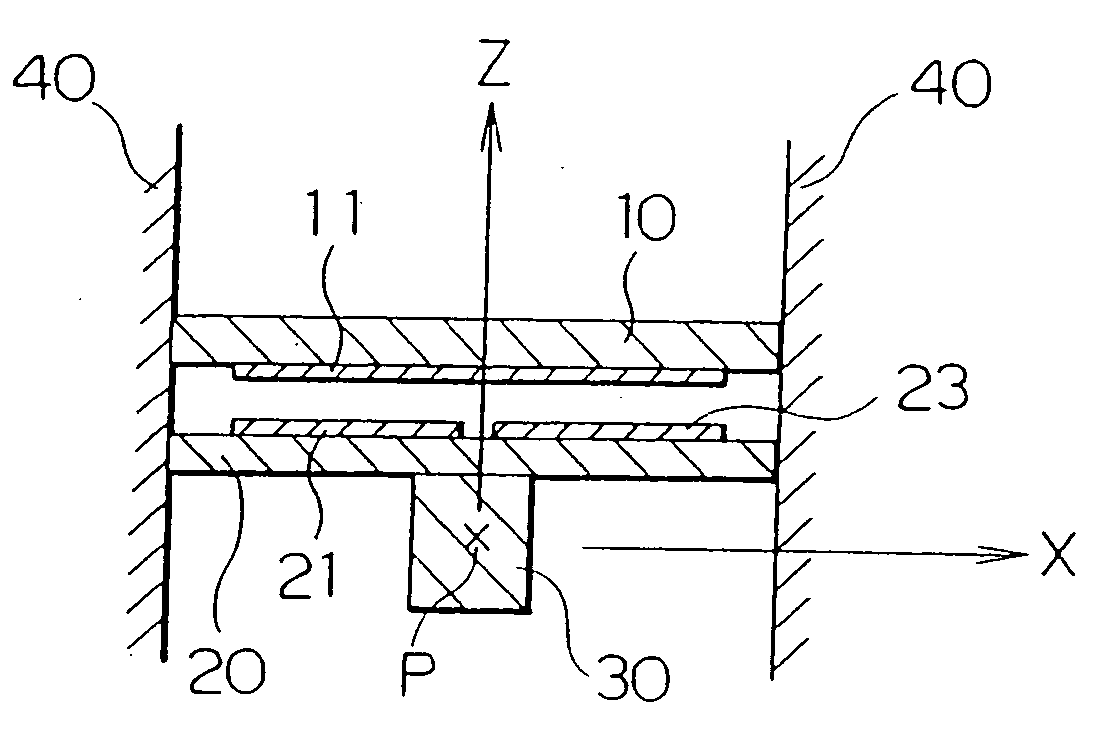
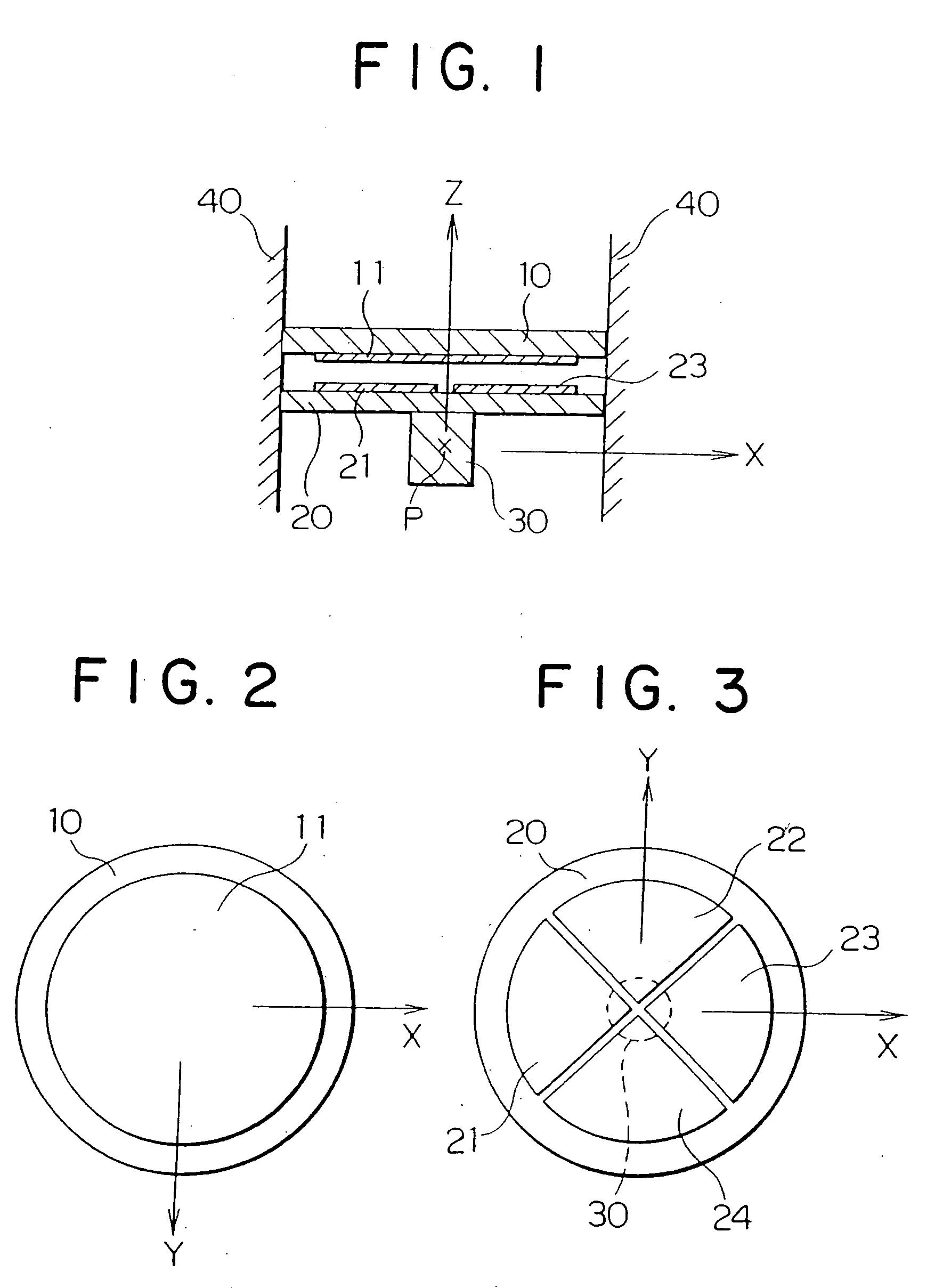
[0129]FIG. 1 is a side cross sectional view showing the structure of an acceleration detector according to a basic embodiment of this invention. This detector comprises, as the major component, a fixed substrate 10, a flexible substrate 20, a working body 30, and a detector casing 40. The bottom view of the fixed substrate 10 is shown in FIG. 2. The cross section cut along the X-axis of the fixed substrate 10 in FIG. 2 is shown in FIG. 1. The fixed substrate 10 is formed as a disk shaped substrate as shown, and is fixed at the peripheral portion thereof to the detector casing 40. On the lower surface thereof, a disk shaped fixed electrode 11 is similarly formed. On the other hand, the top view of the flexible substrate 20 is shown in FIG. 3. The cross section cut along the X-axis of the flexible substrate in FIG. 3 is shown in FIG. 1. The flexible substrate 20 is also formed as a disk shaped substrate as shown, and is fixed at the peripheral portion thereof to the...

5 embodiment

§5 Embodiment Having Test Function

[0156]Generally, in the case of mass producing any detectors to deliver them to the market, the test process is conducted prior to shipping. That is, the work for confirming whether or not the detector normarily carries out the detecting operation is conducted. Also in the previously described acceleration detector, it is preferable to carry out a test prior to shipping. In order to test the acceleration detector, an approach is generally employed to actually apply an acceleration thereto and confirm an electric signal outputted at this time. However, an equipment for producing an acceleration is required for such a test. As a result, the test system becomes large.

[0157]In the embodiment described below, test prior to shipping can be carried out without using such a large test system. FIG. 19 is a side cross sectional view showing the structure of an acceleration detector according to the embodiment having such a test function. This detector compris...


PUM

PropertyMeasurementUnit
temperatureaaaaaaaaaa
capacitanceaaaaaaaaaa
coulomb forceaaaaaaaaaa

Abstract

An electrode layer is formed on the upper surface of a first substrate, and a processing for partially removing the substrate is carried out in order to allow the substrate to have flexibility. To the lower surface of the first substrate, a second substrate is connected. Then, by cutting the second substrate, a working body and a pedestal are formed. On the other hand, a groove is formed on a third substrate. An electrode layer is formed on the bottom surface of the groove. The third substrate is connected to the first substrate so that both the electrodes face to each other with a predetermined spacing therebetween. Finally, the first, second and third substrates are cut off every respective unit regions to form independent sensors, respectively. When an acceleration is exerted on the working body, the first substrate bends. As a result, the distance between both the electrodes changes. Thus, an acceleration exerted is detected by changes in an electrostatic capacitance between both the electrodes.

Description

BACKGROUND OF THE INVENTION[0001]This invention relates to a force detector and an acceleration detector to which the force detector is applied, and more particularly to a detector suitable for detection of multidimensional force or acceleration components. Further, this invention provides a method suitable for mass producing such detectors.[0002]In the automobile industry or the machinery industry, there has been increased demand for detectors capable of precisely detecting a physical quantity such as force, acceleration or magnetism. Particularly, it is required to realize small detectors capable of detecting physical quantities every respective two-dimensional or three-dimensional components.[0003]To meet such a demand, there has been proposed a force detector in which gauge resistors are formed on a semiconductor substrate such as silicon, etc. to transform a mechanical distortion produced in the substrate on the basis of a force applied from the external to an electric signal b...

Claims


Application Information

Patent Timeline
Patent Type & Authority Applications(United States)
IPC IPC(8): G01P15/125B81B3/00G01L1/14G01L5/16G01P15/08G01P15/09G01P15/105G01P15/18
CPCG01L1/144G01L5/165G01L5/167G01P15/0802G01P15/0922Y10S73/04G01P15/125G01P15/18Y10T29/49007Y10T29/43Y10T29/49005G01P15/105G01P2015/084
Inventor OKADA, KAZUHIRO
Owner OKADA KAZUHIRO
Why Eureka
Try Eureka