Liquid crystal panel for liquid crystal display device and the manufacture method of the same

a technology of liquid crystal display device and liquid crystal display device, which is applied in the direction of optics, instruments, chemistry apparatus and processes, etc., can solve the problems of inability to fully electrically connect, inability to achieve full electrical connection, so as to prevent the effect of reducing the yield ra

Inactive Publication Date: 2008-07-31
INFOVISION OPTOELECTRONICS HLDG LTD
View PDF4 Cites 1 Cited by
  • Summary
  • Abstract
  • Description
  • Claims
  • Application Information

AI Technical Summary

Benefits of technology

[0042]According to the invention, in order to utilize effectively the peripheral portion of the liquid crystal panel, the conductive material and BM overlap completely so that the conductivity between the TFT substrate and CF substrate is ensured by the conductive material, mea...

Problems solved by technology

As a result, the portion comprised in the conductive material, which contains the conductive balls, has not been pressed at all, so that the electric connection cannot be obtained between the conductive material and the CF substrate and/or the TFT substrate, or they cannot be fully elect...

Method used


Image

  • Liquid crystal panel for liquid crystal display device and the manufacture method of the same
  • Liquid crystal panel for liquid crystal display device and the manufacture method of the same
  • Liquid crystal panel for liquid crystal display device and the manufacture method of the same

Examples


Embodiment Construction

[0065]The embodiments of the invention will be described by referring to the figures as follows.

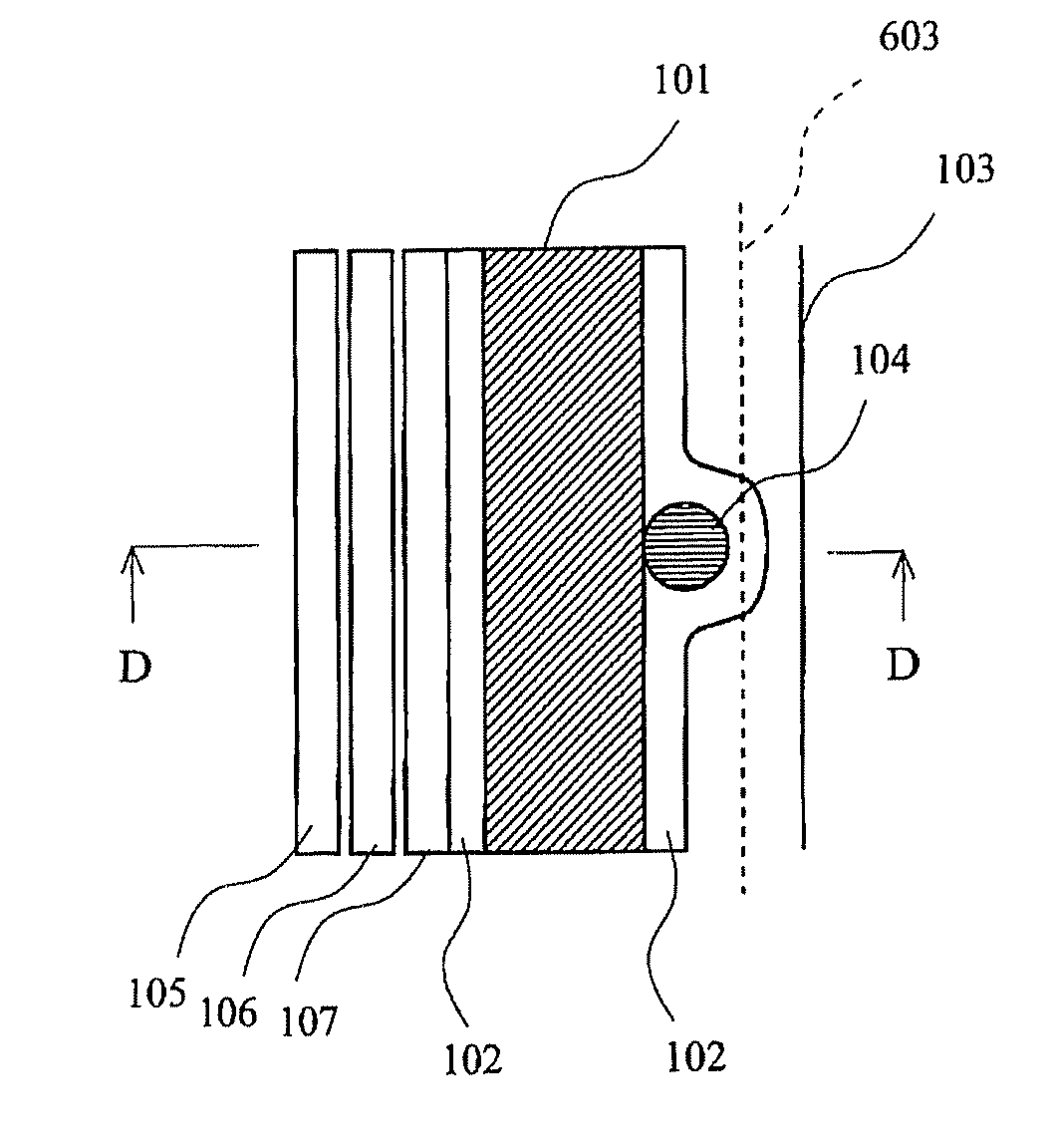
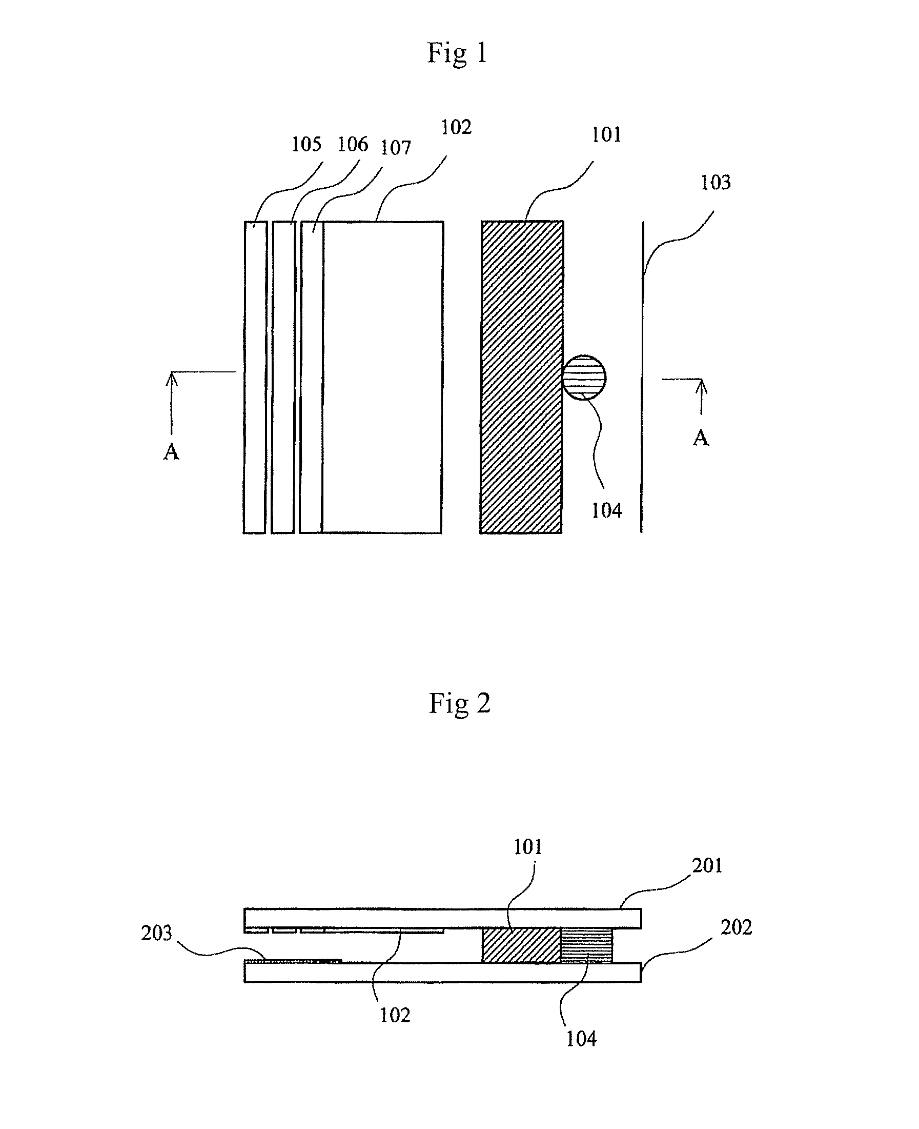
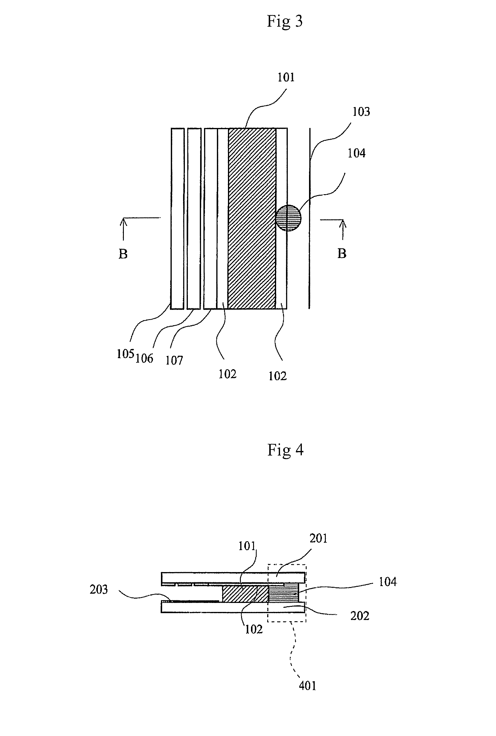
[0066]FIG. 9 is a part plan view illustrating the outline of the liquid crystal panel of an embodiment of the invention. In FIG. 9, 102 is BM, 104 is a conductive material, and 101 is a seal material. FIG. 10 is a cross sectional view taken along the cut off line D-D in FIG. 9.

[0067]In addition, FIG. 11 is an enlarged cross sectional view of the portion 401 in FIG. 10.

[0068]In FIG. 11, D11 is a region where the conductive material 104 is configured under side of the BM 102 in completely superposition.

[0069]In the liquid crystal panel of an embodiment of the invention, the conductive material 104 and the BM 102 overlap completely. Therefore, the thickness of the conductive material 104 positioned between the TFf substrate and the CF substrate is uniform, it can be known from FIG. 11, if the conductive balls 501 are sandwiched between the TFT substrate and the CF substrate to be pressed, th...


PUM

PropertyMeasurementUnit
Electrical conductoraaaaaaaaaa

Abstract

The invention discloses a liquid crystal panel used for liquid crystal display device and a method for manufacturing the same. The object of the invention is to provide a liquid crystal panel having the following structure in order to utilize effectively the peripheral portion of the liquid crystal panel: in a liquid crystal panel which is formed by sandwiching the liquid crystal between a TFT substrate configured with the pixels in a matrix shape and a CF substrate configured with the color filter and sealing the peripheral area with a seal material, the seal material is completely overlappingly disposed on the BM of the CF substrate, and in order to electrically connect said TFT substrate and said CF substrate, a conductive material is adjoined at the outer side of said seal material and is configured to overlap the BM completely, and a structure in which said BM only projects outwardly at the portion, where said conductive material is disposed, is formed. Wherein said conductive material comprises electric transfer isolation component with the electric transfer film disposed on the surface of the isolation component. Therefore, the reduction of the yield rate, which is caused by black matrix being cut off when the cut off line shifts slightly during cutting the substrate, can be decreased while the peripheral portion of the liquid crystal panel substrate is utilized effectively.

Description

FIELD OF THE INVENTION[0001]The invention relates to a liquid crystal panel used for liquid crystal display device and a manufacture method of the same.DESCRIPTION OF THE RELATED ART[0002]In recent years, TFT-LCD (Thin Film Transistor-Liquid Crystal Display) panel has been used widely as the panel of the display of the desktop personal computer and the display device of the notebook personal computer. For the future TFT-LCD, besides it must satisfy the performances required for operating as a display device, the following two points are very important at an aspect of reducing the cost, that is, promoting production efficiency by using larger mother glass substrate and improving effectiveness of batch production by adopting means such as the generalization of components.[0003]Therefore, at an aspect which is indispensable for promoting the production efficiency, that is, at an aspect referred to as “multiple-panel-cutting for cutting a plurality of LCD panels from one mother glass su...

Claims


Application Information

Patent Timeline
IPC IPC(8): B29C65/00
CPCG02F1/1339G02F1/133512
Inventor KAMIYA, HIROYUKIKAMOSHIDA, KENTA
Owner INFOVISION OPTOELECTRONICS HLDG LTD
Why Eureka
Try Eureka