Nitride semiconductor light emitting device
- Summary
- Abstract
- Description
- Claims
- Application Information
AI Technical Summary
Benefits of technology
Problems solved by technology
Method used
Image
Examples
first embodiment
[0041]A first embodiment of the present invention will be described with reference to the accompanying drawings.
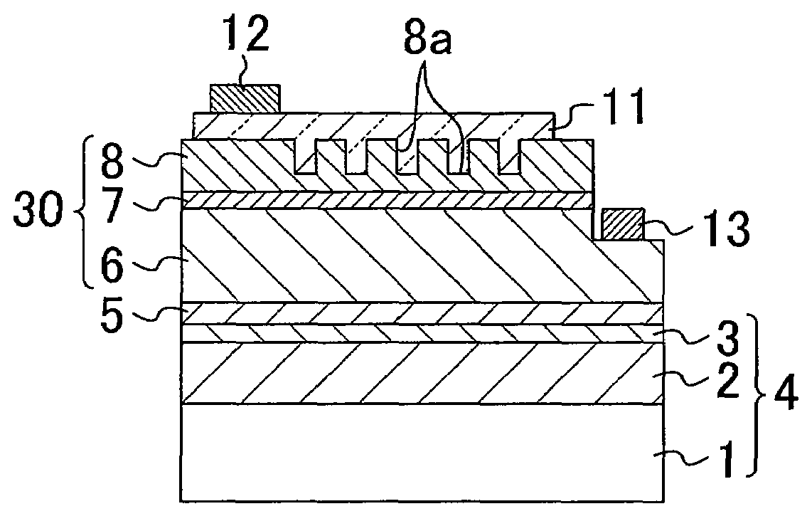
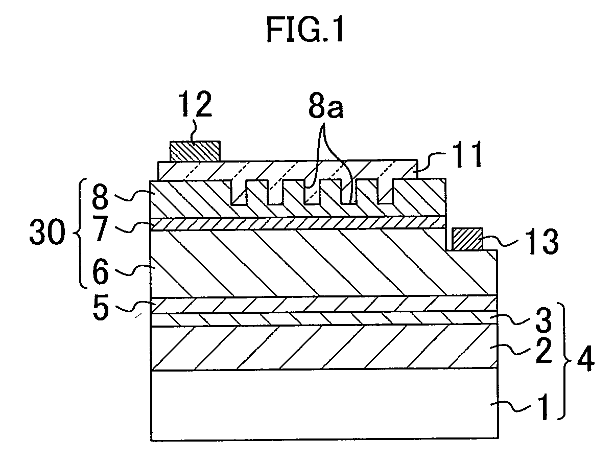
[0042]FIG. 1 shows a cross-sectional structure of a light emitting diode, which is a nitride semiconductor light emitting device according to the first embodiment of the present invention.
[0043]As shown in FIG. 1, a light emitting diode of the first embodiment includes a SOI substrate 4 and a semiconductor laminated body 30 formed of a plurality of nitride semiconductor layers stacked on the SOI substrate 4.
[0044]The SOI substrate 4 includes a substrate (lower silicon layer) 1 formed of silicon (Si), an insulating film (buried insulating layer) 2 formed of, for example, silicon oxide (SiO2) on the substrate 1 and a single crystal thin film (upper single crystal layer) 3 formed of silicon (Si) having a principal surface of a (111) plane orientation on the insulating film 2.
[0045]In forming the SOI substrate 4, the insulating film 2 and the single crystal thin film 3 can be ...
second embodiment
[0065]Hereafter, a second embodiment of the present invention will be described with reference to the accompanying drawings.
[0066]FIG. 4 shows a cross-sectional structure of a light emitting diode, which is a nitride semiconductor light emitting device according to the second embodiment of the present invention. In FIG. 4, each member also shown in FIG. 1 is identified by the same reference numeral and therefore the description thereof will be omitted.
[0067]The light emitting diode of the second embodiment is different from the light emitting diode of the first embodiment in the point that a DBR laminated layer film 16 in which a first semiconductor layer 14 of aluminum nitride (AlN) whose refractivity is 2.14 and a second semiconductor layer 15 of gallium nitride (GaN) whose refractivity is 2.46 are alternately stacked is provided between the buffer layer 5 formed on the SOI substrate 4 and the semiconductor laminated body 30. In this embodiment, the DBR laminated layer film 16 is ...
third embodiment
[0076]Hereafter, a third embodiment of the present invention will be described with reference to the accompanying drawings.
[0077]FIG. 7A is a plan view illustrating a structure of a surface emitting laser device, which is a nitride semiconductor light emitting device according to the third embodiment of the present invention. FIG. 7B is a cross-sectional view taken along the line VIIb-VIIb of FIG. 7A. In the FIGS. 7A and 7B, each member also shown in FIG. 1 is identified by the same reference numeral and therefore the description thereof will be omitted.
[0078]As shown in FIG. 7B, the nitride semiconductor light emitting device of the third embodiment is a surface emitting laser device including a first DBR laminated layer film 17 formed of nitride semiconductor formed between a buffer layer 5 and a semiconductor laminated body 30 and having a DBR mirror structure and a second DBR laminated layer film 20 formed on the p-type cladding layer 8 and having a DBR mirror structure in which...
PUM
 Abstract
Description
Claims
Application Information
 - R&D
- Intellectual Property
- Life Sciences
- Materials
- Tech Scout
- Unparalleled Data Quality
- Higher Quality Content
- 60% Fewer Hallucinations
Browse by: Latest US Patents, China's latest patents, Technical Efficacy Thesaurus, Application Domain, Technology Topic, Popular Technical Reports.
© 2025 PatSnap. All rights reserved.Legal|Privacy policy|Modern Slavery Act Transparency Statement|Sitemap|About US| Contact US: help@patsnap.com


