Semiconductor device and method of manufacturing the same

Inactive Publication Date: 2008-08-07
ABLIC INC
View PDF1 Cites 22 Cited by
  • Summary
  • Abstract
  • Description
  • Claims
  • Application Information

AI Technical Summary

Benefits of technology

[0040]Lamination of a resistor and a fuse element permits formation of a semiconductor device having the resistor and the fuse element connected in parallel and a smaller area compared to a conventional semiconductor device. By applying the semiconductor device according to the present invention to a bleeder resistance circuit, which is formed of two or more resistors each connected in parallel with a fuse element and capable of adjusting voltage output divided

Problems solved by technology

Though electrical connection between the first polycrystalline silicon film 301 and the second polycrystalline silicon film 302 is made through their mutual contact, there is a problem

Method used


Image

  • Semiconductor device and method of manufacturing the same
  • Semiconductor device and method of manufacturing the same
  • Semiconductor device and method of manufacturing the same

Examples


Example

[0053]Hereinafter, a preferred embodiment of a semiconductor device according to the present invention will be described in detail with reference to the attached drawings.

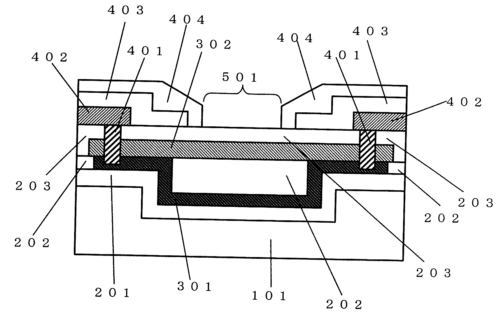
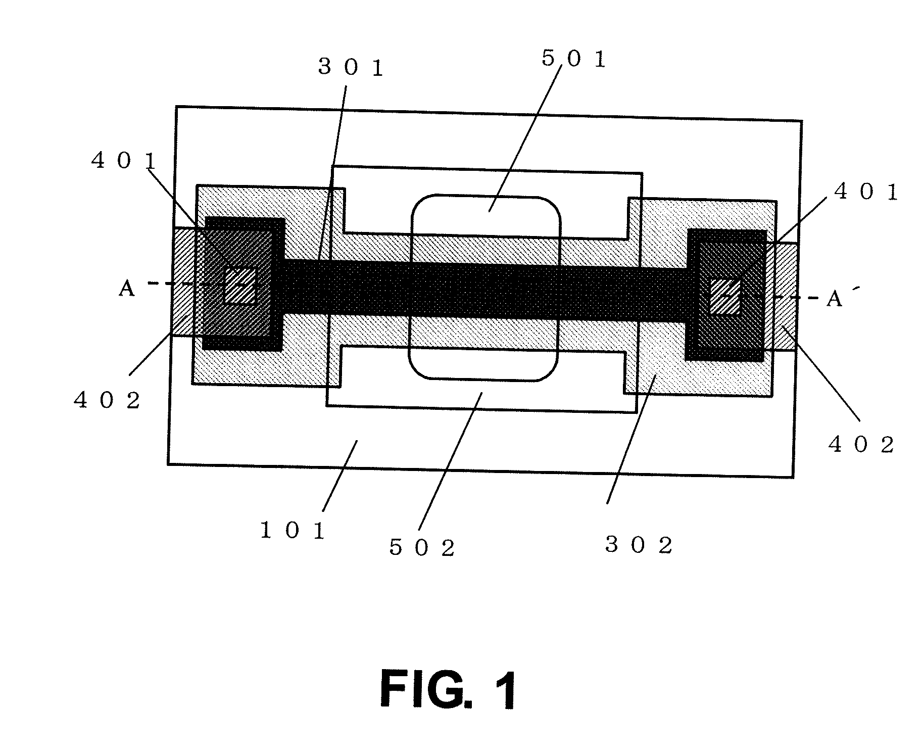
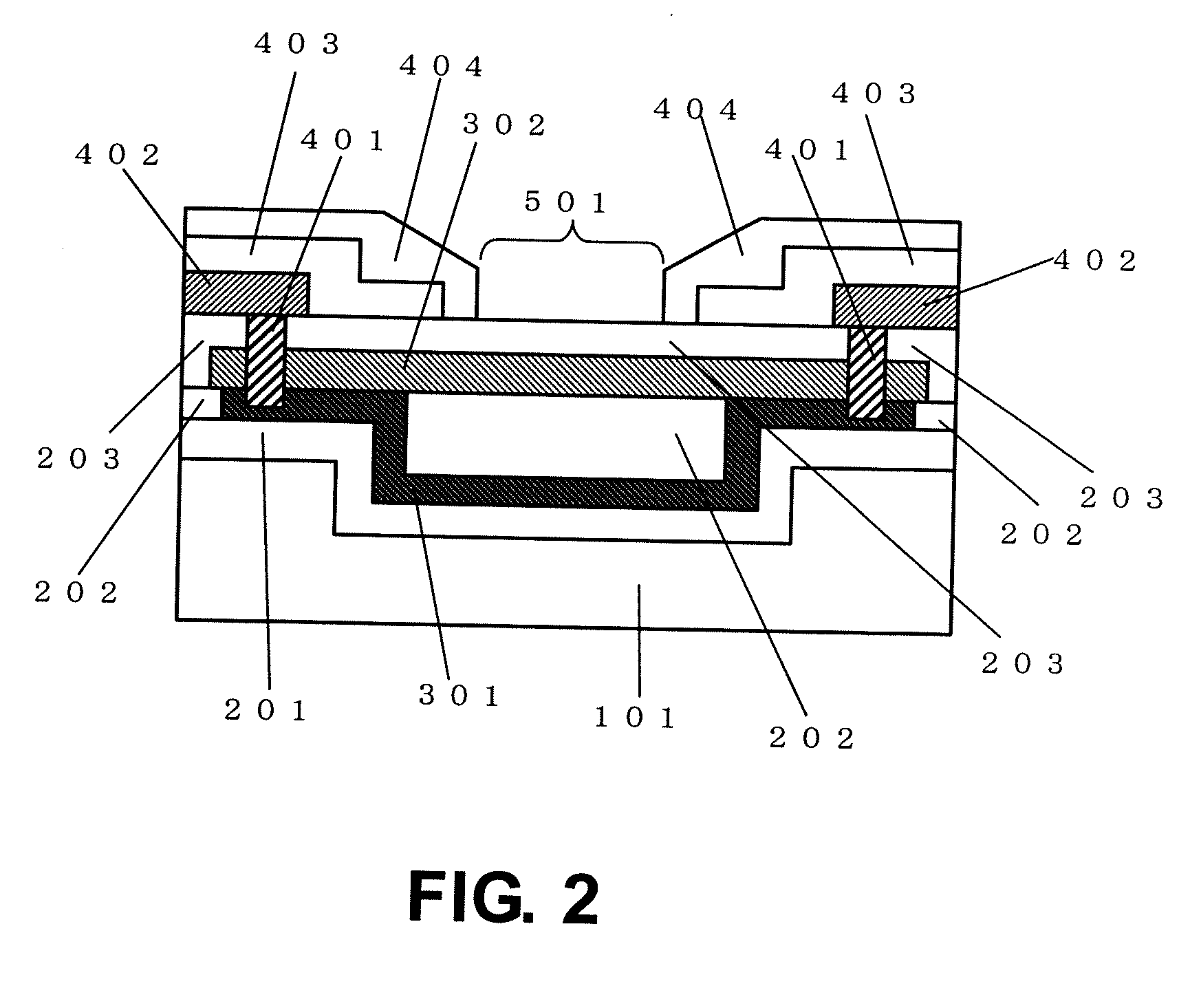
[0054]FIG. 1 is an example of a plan view of a semiconductor device according to an embodiment of the present invention. FIG. 2 is an exemplary sectional view taken along the line A-A′ of FIG. 1 of the semiconductor device according to the embodiment of the present invention.

[0055]As illustrated in FIG. 1, a resistor formed of a first polycrystalline silicon film 301 is formed on a trench region 502. Laminated to the resistor, a fuse element formed of a second polycrystalline silicon film 302 is formed. The resistor, the fuse element, and metal interconnect 402 are electrically connected via a plug 401. A region 501 for cutting the fuse element is formed at the center of the fuse element where the fuse element is to be cut later with a laser.

[0056]As illustrated in FIG. 2, the resistor formed of the first polycryst...


PUM


Abstract

A fuse element is laminated on a resistor and the resistor is formed in a concave shape below a region in which cutting of the fuse element is carried out with a laser. Accordingly, there can be provided a semiconductor device which occupies a small area, causes no damage on the resistor in the cutting of the fuse element, has a small contact resistance occurred between elements, and has stable characteristics, and a method of manufacturing the same.

Description

[0001]This application claims priority under 35 U.S.C. §119 to Japanese Patent application No. JP2007-028297 filed Feb. 7, 2007, the entire content of which is hereby incorporated by reference.TECHNICAL FIELD[0002]The present invention relates to a semiconductor device in which a resistor and a fuse element are connected in parallel and a resistance value can be adjusted by cutting the fuse element, a semiconductor device having a bleeder resistance circuit which can, by cutting fuse elements which are connected in parallel with two or more resistors, respectively, adjust voltage output divided by the resistors, and a method of manufacturing the same.BACKGROUND ART[0003]When the resistor and the fuse element are formed in the same layer in a semiconductor device in which a resistor formed of a polycrystalline silicon film and a fuse element are electrically connected in parallel, two elements have to be arranged in the same plane, causing an increase in chip area. One way to solve t...

Claims


Application Information

Patent Timeline
IPC IPC(8): H01L29/00H01L21/02
CPCH01L28/20
Inventor KITAJIMA, YUICHIRO
Owner ABLIC INC
Why Eureka
Try Eureka