Power conversion apparatus

a technology of power conversion apparatus and power conversion device, which is applied in the direction of electrical apparatus construction details, basic electric elements, solid-state devices, etc., can solve the problems of suppressing this temperature increase and large amount of heat generation, and achieve the enhancement of cooling capability, the effect of reducing the size of the semiconductor module, and enhancing the cooling efficiency of the semiconductor chip constituting the inverter circui

Active Publication Date: 2008-08-07
HITACHI ASTEMO LTD
View PDF2 Cites 87 Cited by
  • Summary
  • Abstract
  • Description
  • Claims
  • Application Information

AI Technical Summary

Benefits of technology

[0052]According to the present invention, the cooling efficiency of a semiconductor chip constituting an inverter circuit can be enhanced. This enhancement of

Problems solved by technology

A large amount of heat is generated at the power semiconductor when performing the chang

Method used


Image

  • Power conversion apparatus
  • Power conversion apparatus
  • Power conversion apparatus

Examples


Embodiment Construction

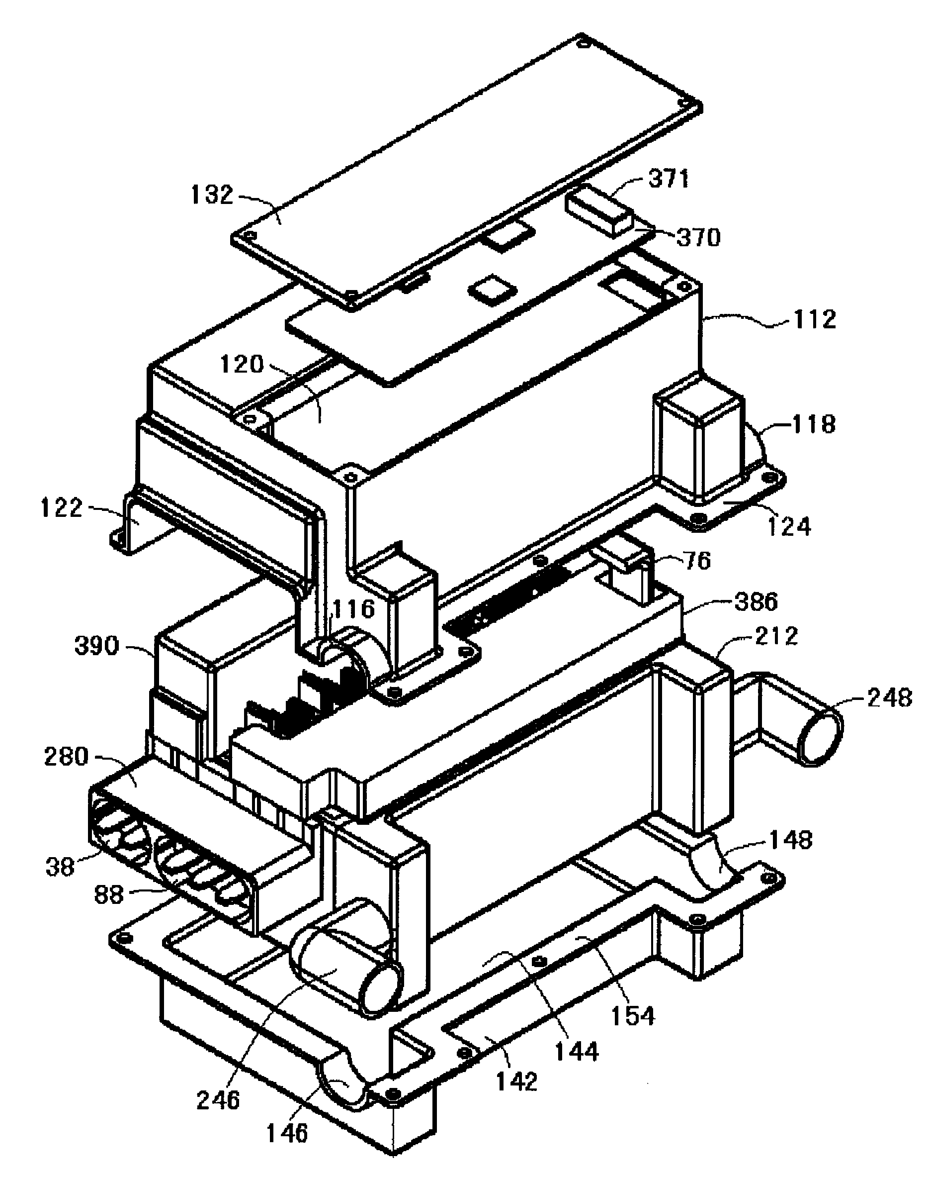
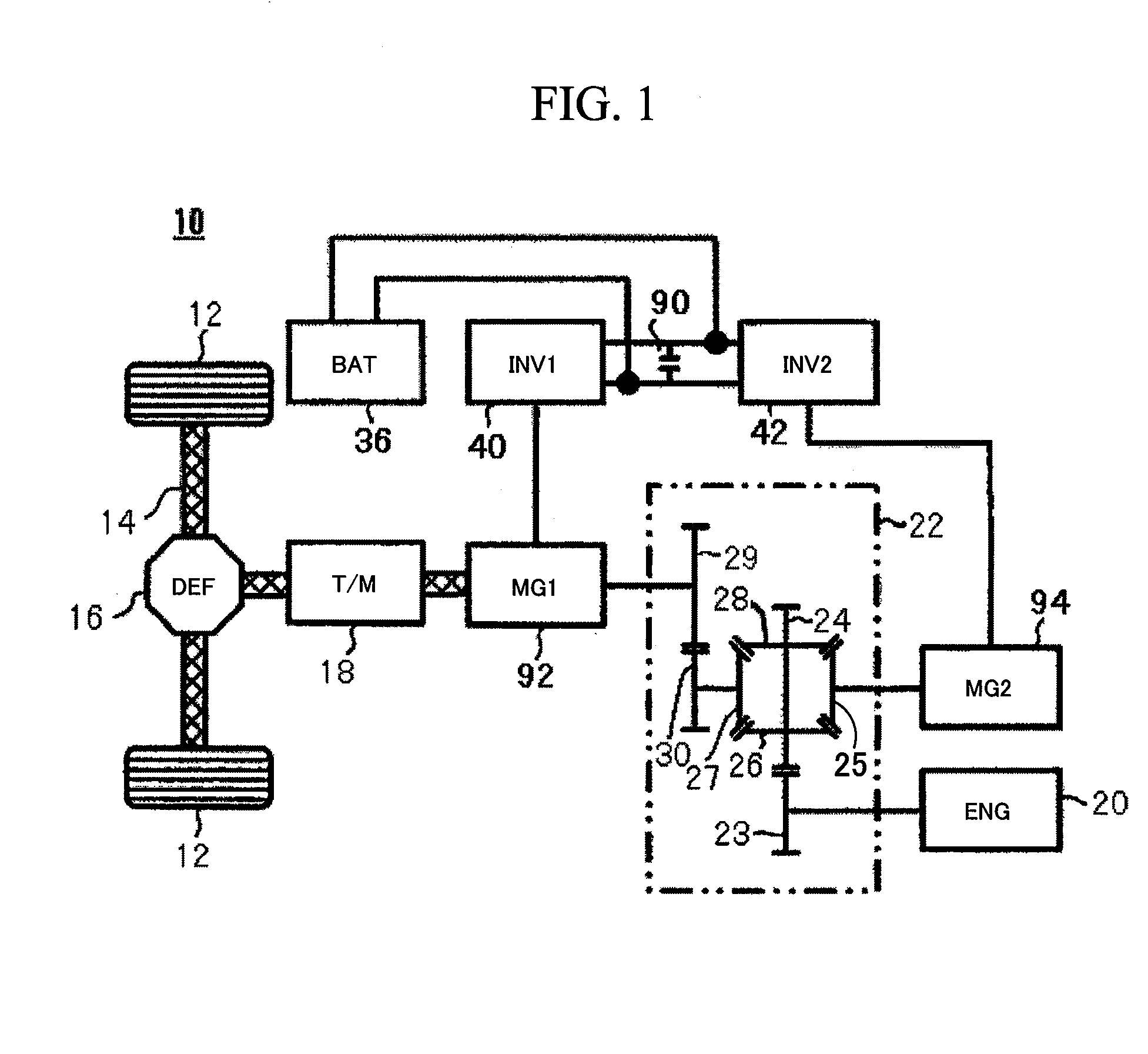
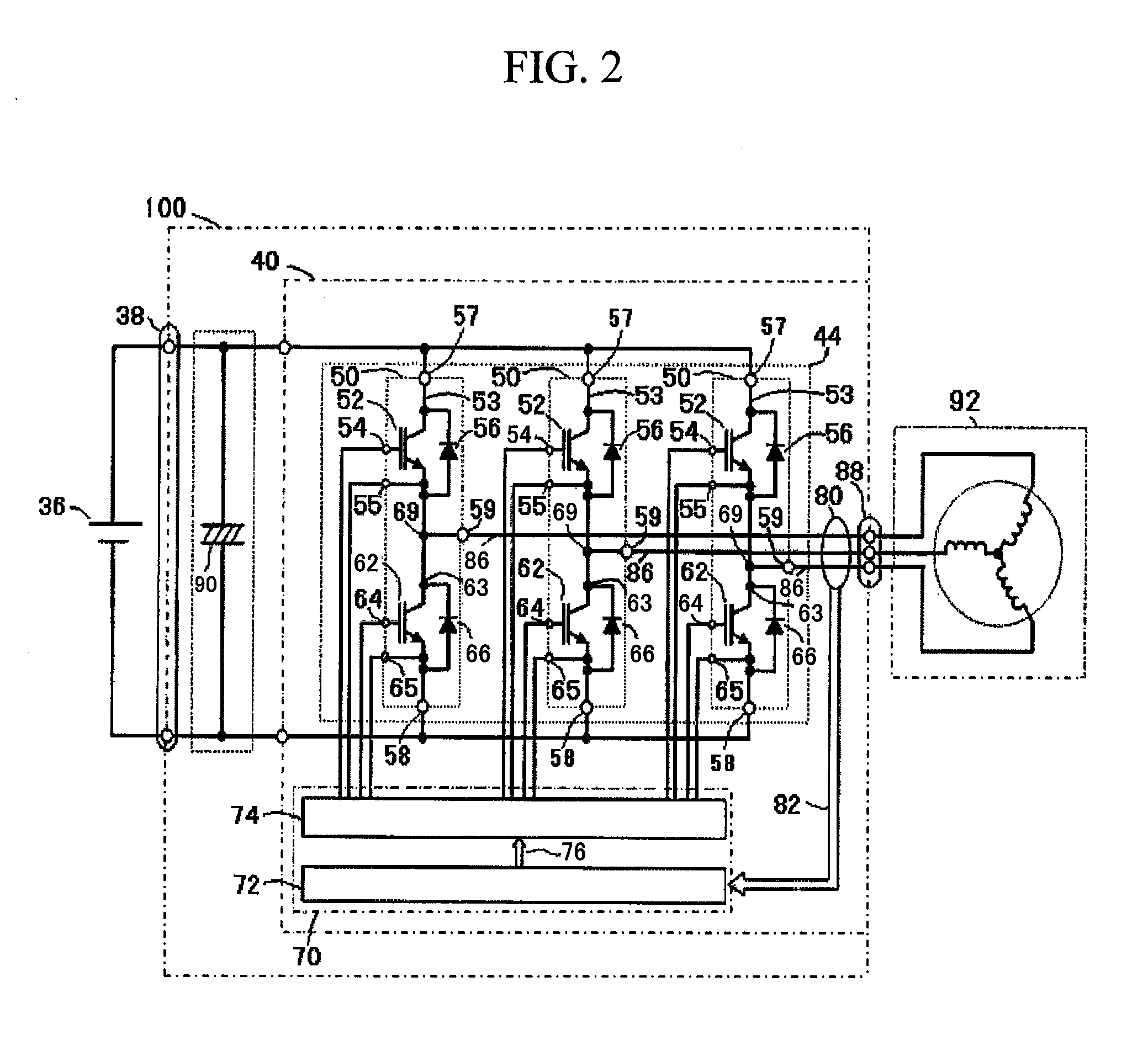
[0096]The power conversion apparatus according to the embodiment of the present invention is described below in detail while referring to the drawings. However, first, an overview of technical problems to be overcome and improved in regard to the power conversion apparatus according to the embodiment and technology for solving the technical problems are described.

[0097]The power conversion apparatus according to the embodiment of the present invention has been made in consideration of the following technical aspects as a product that can respond to the needs of the marketplace. One of those aspects is size-reduction technology, that is, technology that inhibits as much as possible an increase in size of a power conversion apparatus accompanying an increase in the amount of power that is converted. Another aspect is technology that relates to improving the reliability of a power conversion apparatus. A further aspect is technology that relates to improving the productivity of a power...


PUM


Abstract

Technology leading to a size reduction in a power conversion apparatus comprising a cooling function and technology relating to enhancing productivity and enhancing reliability necessary for commercial production are provided. Series circuits comprising an upper arm and lower arm of an inverter circuit are built in a single semiconductor module 500. The semiconductor module has cooling metal on two sides. An upper arm semiconductor chip and lower arm semiconductor chip are wedged between the cooling metals. The semiconductor module is inserted inside a channel case main unit 214. A DC positive electrode terminal 532, a DC negative electrode terminal 572, and an alternating current terminal 582 of a semiconductor chip are disposed in the semiconductor module. The DC terminals 532 and 572 are electrically connected with a terminal of a capacitor module. The alternating current terminal 582 is electrically connected with a motor generator via an AC connector.

Description

BACKGROUND OF THE INVENTION[0001]1. Field of the Invention[0002]The present invention relates to a power conversion apparatus comprising an inverter circuit.[0003]2. Background Art[0004]As conventional technology that is designed to improve heat dissipation properties by efficiently conducting heat from a semiconductor module to a cooler, for example, a cooling structure disclosed in JP Patent Publication (Kokai) No. 2005-175163A has been proposed. According to JP Patent Publication (Kokai) No. 2005-175163A, a semiconductor module is inserted into a hole for module insertion that is formed at a cooler to dissipate heat from an abutting surface of the hole for module insertion. The surface that abuts with the hole for module insertion of the semiconductor module is coated with a soft metal layer to dissipate heat to the cooler through the soft metal layer.[0005]Further, as conventional technology designed to achieve compatibility between assemblability and cooling efficiency of a sem...

Claims


Application Information

Patent Timeline
IPC IPC(8): H02M7/537H05K7/20
CPCH01L23/473H01L2924/3011H05K7/20927H02M7/537H02M7/5387H01L2924/0002H05K7/209H01L2924/00H02M7/003H01L23/50
Inventor TOKUYAMA, TAKESHINAKATSU, KINYASAITO, RYUICHI
Owner HITACHI ASTEMO LTD
Why Eureka
Try Eureka