Plasma etching method, plasma etching apparatus, control program and computer-readable storage medium

a plasma etching and plasma technology, applied in the direction of electrical devices, decorative surface effects, decorative arts, etc., can solve the problems of reducing the yield, xe gas is expensive, and it is difficult to perform the desired plasma etching, so as to increase the manufacturing cost and improve the yield of superior goods

Active Publication Date: 2008-08-14
TOKYO ELECTRON LTD
View PDF3 Cites 4 Cited by
  • Summary
  • Abstract
  • Description
  • Claims
  • Application Information

AI Technical Summary

Benefits of technology

[0007]In view of the foregoing, the present invention provides a plasma etching method and apparatus capable of improving a production yield with no increase in manufacturing costs by preventing a mask collapse without using Xe gas, even when forming a hole having a high aspect ratio. Further, the present invention provides a control program and a computer-readable storage medium to be used therefor.
[0016]In accordance with an embodiment of the present invention, since the mask collapse can be restricted without using Xe gas even when forming holes of a high aspect ratio, the plasma etching method, the plasma etching apparatus, a control program, and a computer readable storage medium for improving the yield of superior goods without increasing manufacturing costs can be provided.

Problems solved by technology

As described above, in the plasma etching process performed by using the multi-layer resist mask, in a case where holes are formed in a silicon oxide film and a glass based film formed under the silicon oxide film by using a gaseous mixture of C4F6 gas, Ar gas, and O2 gas, there is a problem that when an aspect ratio is increased, the frequency of occurrence of the so-called “mask collapse”, wherein the resist mask falls down during the etching process increases, thereby making it impossible to perform the desired plasma etching and eventually leading to a reduction of the yield.
Since, however, Xe gas is expensive, there is still a problem that manufacturing costs for the semiconductor devices are increased when using Xe gas.

Method used


Image

  • Plasma etching method, plasma etching apparatus, control program and computer-readable storage medium
  • Plasma etching method, plasma etching apparatus, control program and computer-readable storage medium
  • Plasma etching method, plasma etching apparatus, control program and computer-readable storage medium

Examples


Embodiment Construction

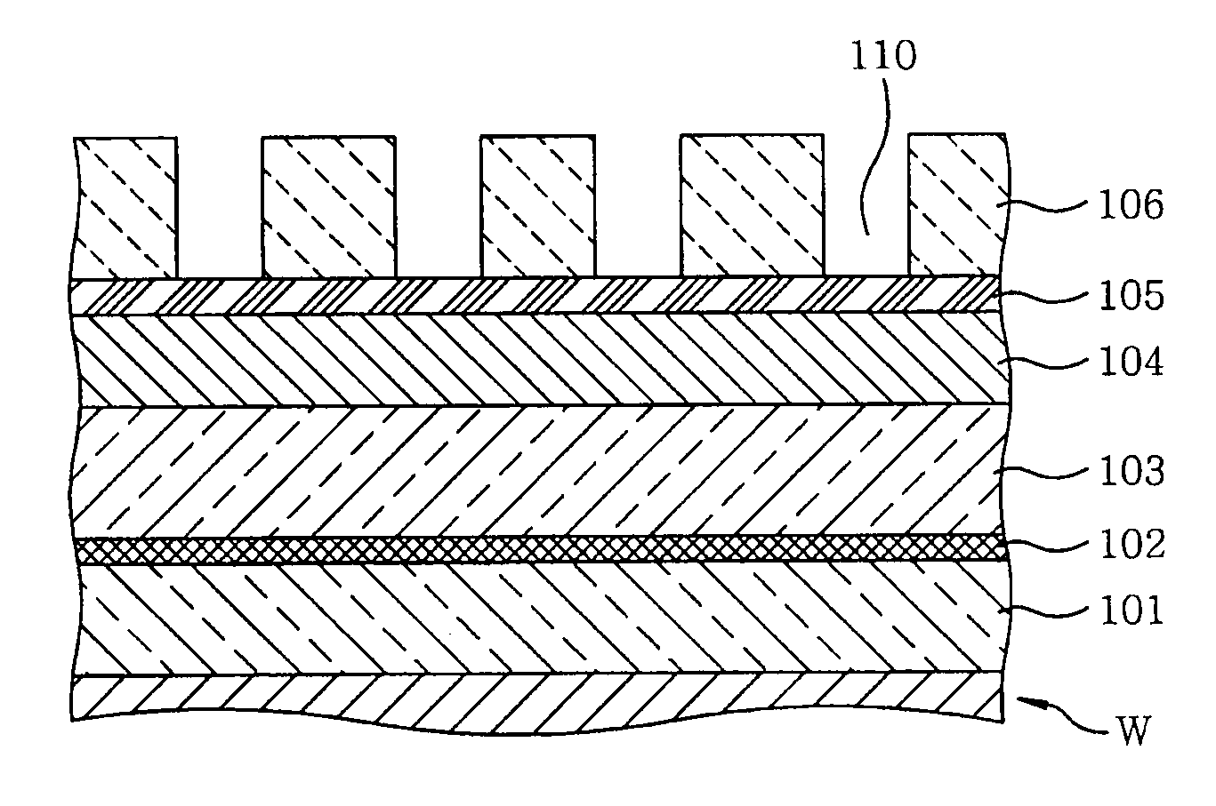
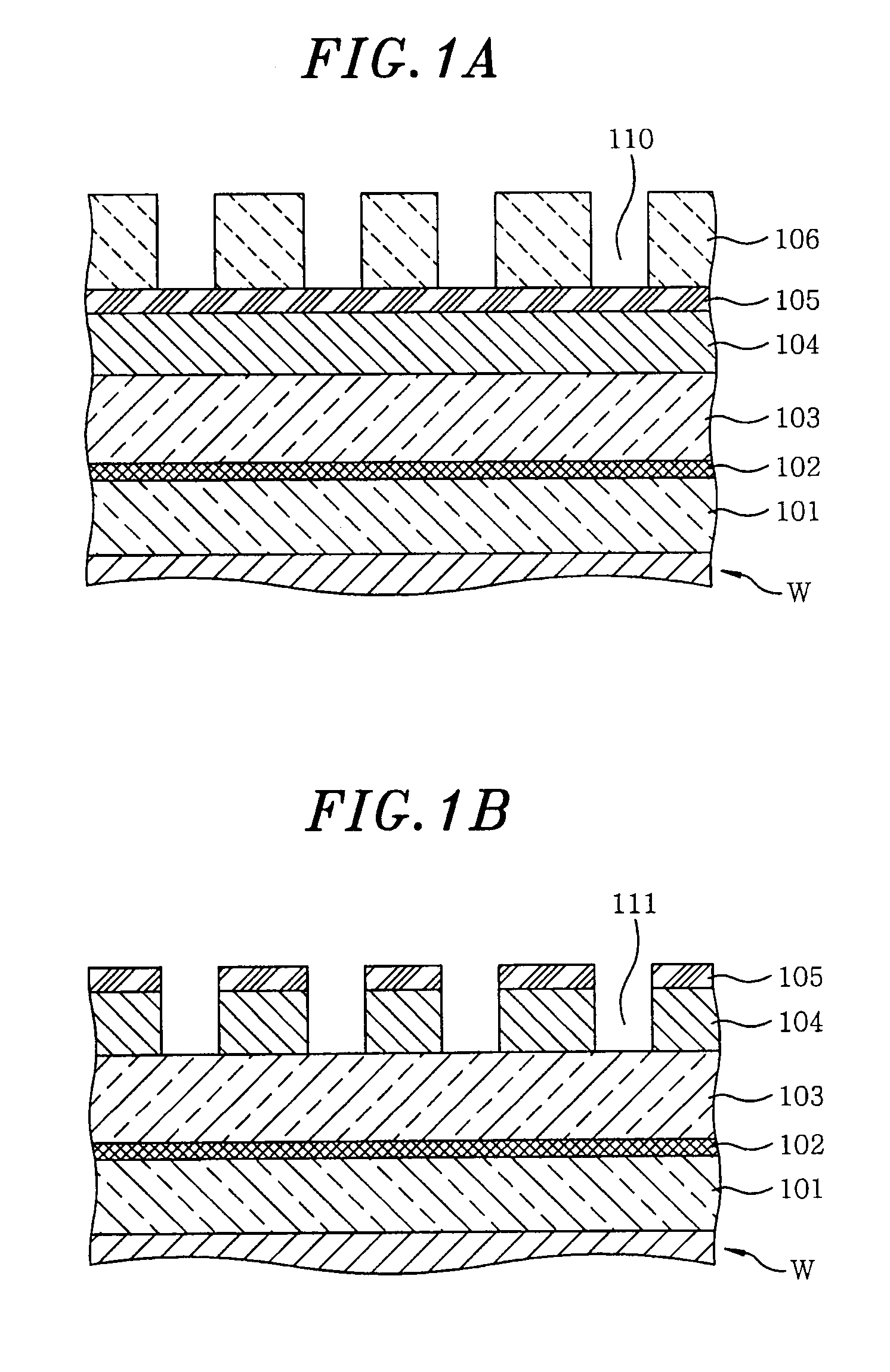
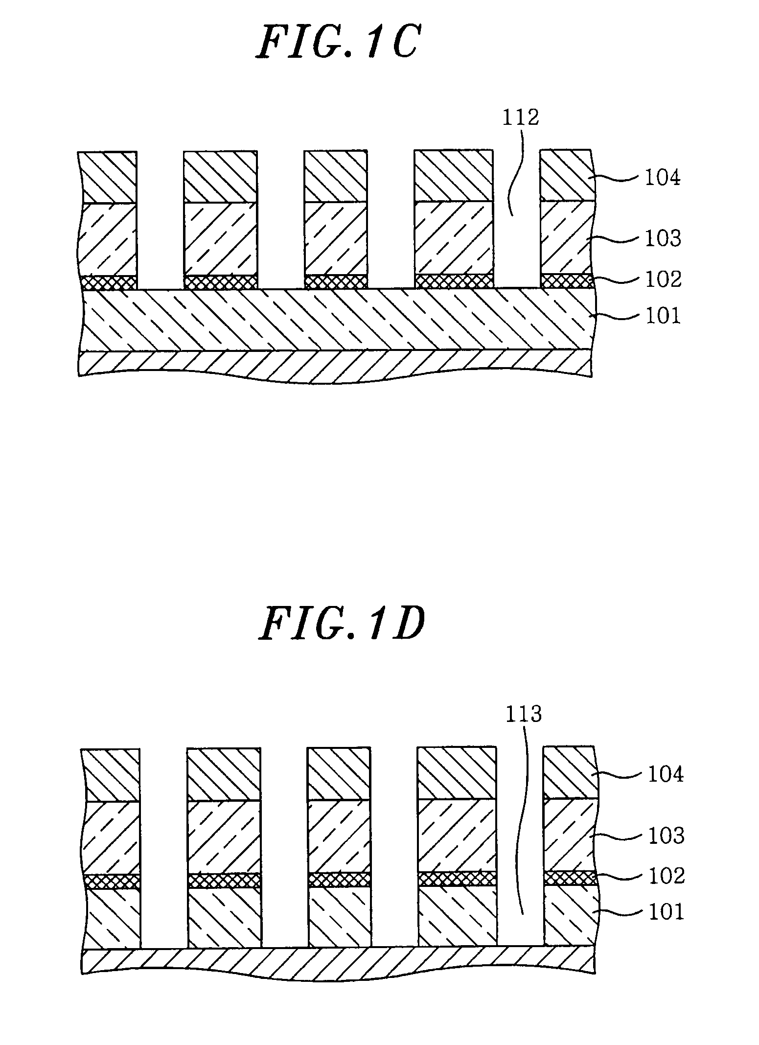
[0022]Hereinafter, an embodiment of the present invention will be described in detail with reference to the accompanying drawings. FIGS. 1A to 1D are enlarged cross sectional views illustrating a semiconductor wafer as a substrate to be processed in a plasma etching method in accordance with the embodiment of the present invention. FIG. 2 is a view illustrating a configuration of a plasma etching apparatus in accordance with the embodiment of the present invention. First, the plasma etching apparatus will be described with reference to FIG. 2.

[0023]The plasma etching apparatus includes a processing chamber 1 which is airtightly configured and electrically grounded. The processing chamber 1 has a cylindrical shape and is made of, e.g., aluminum. In the processing chamber 1, a mounting table 2 is provided to horizontally sustain a semiconductor wafer W, which is a target substrate. The mounting table 2, which is made of, e.g., aluminum, is supported by a conductive support 4 via an in...


PUM

PropertyMeasurementUnit
aspect ratioaaaaaaaaaa
frequencyaaaaaaaaaa
frequencyaaaaaaaaaa

Abstract

A plasma etching method includes: plasma etching a silicon oxide film to be etched that is positioned under a multi-layer resist mask by using the multi-layer resist mask formed on a substrate to be processed; and plasma etching a glass based film positioned under the silicon oxide film by using the multi-layer resist mask. In the method a gaseous mixture of C4F6 gas and C3F8 gas as a processing gas is used in the plasma etching of the glass based layer.

Description

FIELD OF THE INVENTION[0001]The present invention relates to a plasma etching method and apparatus for plasma etching first a silicon oxide film formed under a multi-layer resist film by using the multi-layer resist film as a mask, and then, subsequently plasma etching a glass based film formed under the silicon oxide film by using a multi-layer resist film as a mask; and also relates to a control program and a computer-readable storage medium to be used therefor.BACKGROUND OF THE INVENTION[0002]Conventionally, in a manufacturing process for a semiconductor device, a plasma etching process is performed via a resist mask to form a silicon oxide film or a glass based film (e.g., a BPSG film, a PSG film and the like) after a desired pattern. Further in such a plasma etching method, there is known a technique for performing micro-processing with a high accuracy by using a multi-layer resist mask.[0003]Moreover, when plasma etching a glass based film, there is known a method in which a g...

Claims


Application Information

Patent Timeline
Patent Type & Authority Applications(United States)
IPC IPC(8): C03C15/00H01L21/306
CPCH01L21/31116H01L21/67069H01L21/31144
Inventor LEE, SUNG TAE
Owner TOKYO ELECTRON LTD
Why Eureka
Try Eureka