
Semiconductor device comprising electromigration prevention film and manufacturing method thereof

Active Publication Date: 2008-08-14
AOI ELECTRONICS CO LTD
View PDF7 Cites 18 Cited by
  • Summary
  • Abstract
  • Description
  • Claims
  • Application Information

AI Technical Summary

Benefits of technology

[0008]It is therefore an object of this invention to provide a semiconductor device and a manufacturing method thereof which can prevent a short circuit caused between wiring lines by electromigration and which makes it possible to prevent the wiring lines from being easily mechanically damaged by fillers even if a resin containing the fillers is used as the material of a sealing film.
[0039]According to the present inventions, the electromigration prevention film is provided on at least the surfaces of the wiring lines, and it is therefore possible to prevent a short circuit caused between the wiring lines by electromigration. Moreover, the electromigration prevention film functions as a protective film, which makes it possible to prevent the wiring lines from being easily mechanically damaged by fillers even if a resin containing the fillers is used as the material of the sealing film.

Problems solved by technology

In the conventional semiconductor device described above, the sealing film directly covering the wiring lines is formed of an epoxy resin, so that there is such a problem that metal (copper) ions in the wiring lines diffuse into the sealing film due to the generation of electromigration, which is one factor of a short circuit caused between the wiring lines.
In such a semiconductor device, the wiring lines may be mechanically damaged by the fillers.
In preventing the breaking of the wiring lines due to the mechanical damage, there is a problem of a limit in the miniaturization of the wiring lines.

Method used


Image

  • Semiconductor device comprising electromigration prevention film and manufacturing method thereof
  • Semiconductor device comprising electromigration prevention film and manufacturing method thereof
  • Semiconductor device comprising electromigration prevention film and manufacturing method thereof

Examples


first embodiment

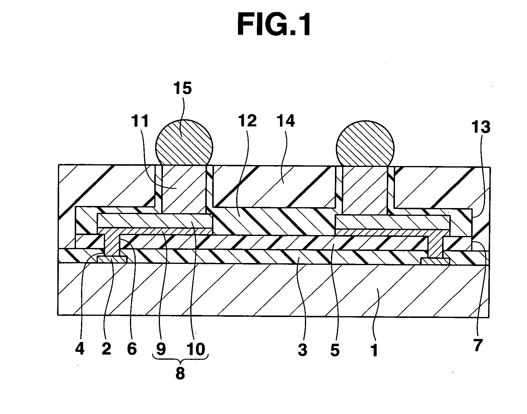
[0076]FIG. 1 shows a sectional view of a semiconductor device as a first embodiment of this invention. This semiconductor device is called a CSP, and comprises a silicon substrate (semiconductor substrate) 1. An integrated circuit (not shown) is provided on or in the upper surface of the silicon substrate 1, and a plurality of connection pads 2 made of a metal such as an aluminum-based metal are provided in peripheral parts of the upper surface of the silicon substrate 1 so that these connection pads are electrically connected to the integrated circuit.

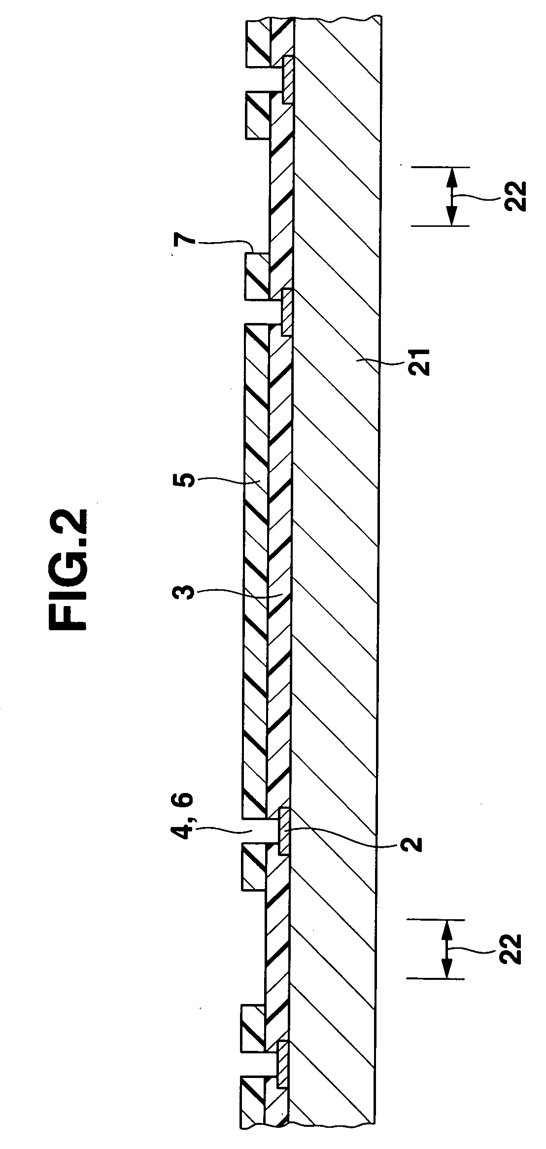
[0077]An insulating film 3 made of an inorganic material such as silicon oxide or silicon nitride is provided on the upper surfaces of the connection pads 2 except for the centers of the connection pads 2 and on the upper surface of the silicon substrate 1. The centers of the connection pads 2 are exposed via openings 4 provided in the insulating film 3. An electrically insulating protective film 5 made of an organic material such as ...

second embodiment

[0094]FIG. 11 shows a sectional view of a semiconductor device as a second embodiment of this invention. This semiconductor device is different from the semiconductor device shown in FIG. 1 in that the lower outer peripheral surface of a columnar electrode 11 is covered with an electromigration prevention film 12, and that the upper outer peripheral surface of the columnar electrode 11 is covered with a sealing film 14 so that the upper surfaces of the cylindrical portions of the electromigration prevention film 12 are not exposed in the upper surface of the sealing film 14.

[0095]Next, one example of a method of manufacturing this semiconductor device will be described. In this case, after the step shown in FIG. 6, a resist film 41 is formed by, for example, a spin coat method on the upper surface of an insulating film 3 exposed by recesses or grooves 7, 13 of a protective film 5 and the electromigration prevention film 12 and on the upper surfaces of parts of the electromigration p...

third embodiment

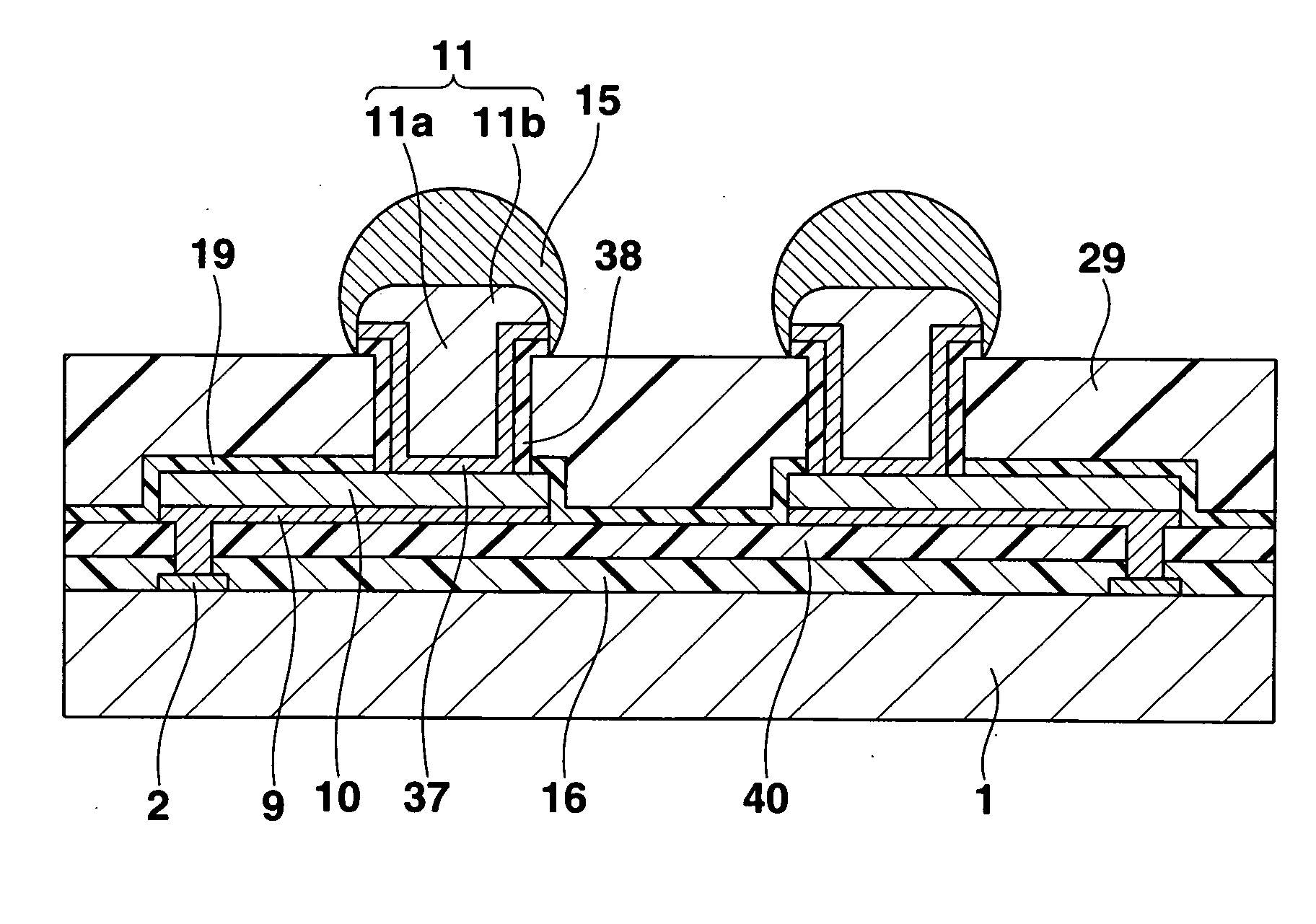
[0098]FIG. 14 shows a sectional view of a semiconductor device as a third embodiment of this invention. This semiconductor device is called a CSP, and comprises a silicon substrate (semiconductor substrate) 1. An integrated circuit (not shown) is provided on the upper surface of the silicon substrate 1, and a plurality of connection pads 2 made of a metal such as an aluminum-based metal are provided in peripheral parts of the upper surface of the silicon substrate 1 so that these connection pads are connected to the integrated circuit.

[0099]A first inorganic insulating film 16 made of an inorganic material containing silicon oxide or silicon nitride as the main component is provided on the upper surfaces of connection pads 2 except for the centers of the connection pads 2 and on the upper surface of the silicon substrate 1. The centers of the connection pads 2 are exposed via openings 4 provided in the first inorganic insulating film 16. An organic protective film (organic insulatin...


PUM


Abstract

A semiconductor device includes a semiconductor substrate, a plurality of wiring lines which are provided on one side of the semiconductor substrate and which have connection pad portions, and a plurality of columnar electrodes respectively provided on the connection pad portions of the wiring lines, each of the columnar electrodes including an outer peripheral surface and a top surface. An electromigration prevention film is provided on at least the surfaces of the wiring lines. A sealing film is provided around the outer periphery surfaces of the columnar electrodes.

Description

CROSS-REFERENCE TO RELATED APPLICATIONS[0001]This application is based upon and claims the benefit of priority from prior Japanese Patent Applications No. 2007-014533, filed Jan. 25, 2007; and No. 2007-086418, filed Mar. 29, 2007, the entire contents of both of which are incorporated herein by reference.BACKGROUND OF THE INVENTION[0002]1. Field of the Invention[0003]This invention relates to a semiconductor device comprising an electromigration prevention film and a manufacturing method thereof.[0004]2. Description of the Related Art[0005]A semiconductor device called a chip size package (CSP) has been described in Jpn. Pat. Appln. KOKAI Publication No. 2004-207306. This semiconductor device comprises a semiconductor substrate having a plurality of connection pads provided on its upper surface. On the upper surface of an insulating film provided on the semiconductor substrate, a plurality of wiring lines are provided so that they are electrically connected to the respective connecti...

Claims


Application Information

Patent Timeline
IPC IPC(8): H01L23/48
CPCH01L2224/05624H01L2224/05647H01L2924/01033H01L2924/01006H01L2924/00013H01L2224/05083H01L2224/0401H01L2224/1147H01L2224/1148H01L2224/13006H01L2224/13022H01L2224/131H01L2224/16H01L2924/01013H01L2924/01014H01L2924/01015H01L2924/01022H01L2924/01029H01L2924/01047H01L2924/01078H01L2924/014H01L2924/05042H01L2924/14H01L2924/30107H01L24/03H01L24/05H01L24/11H01L24/12H01L2224/0231H01L2224/13099H01L2224/29099H01L2224/05024H01L2224/05008H01L2224/05022H01L2224/05001H01L2224/05572H01L2224/05111H01L2224/05124H01L2224/05147H01L2224/05166H01L2224/0236H01L2224/02126H01L2924/00014H01L23/485
Inventor KOUNO, ICHIROWAKABAYASHI, TAKESHIMIHARA, ICHIRO
Owner AOI ELECTRONICS CO LTD
Features
  • Generate Ideas
  • Intellectual Property
  • Life Sciences
  • Materials
  • Tech Scout
  • Unparalleled Data Quality
  • Higher Quality Content
  • 60% Fewer Hallucinations
Learn More