Method of forming one or more nanopores for aligning molecules for molecular electronics

a technology of molecular electronics and nanopores, which is applied in the field of nanopores useful for aligning molecules, can solve the problems of limiting the depth of the hole, difficult control of the orientation of the molecules, and inability to easily achieve langmuir-blodgett techniques, etc., and achieves the effect of less sensitive to the particular molecul

Inactive Publication Date: 2008-08-28
HEWLETT PACKARD DEV CO LP
View PDF5 Cites 6 Cited by
  • Summary
  • Abstract
  • Description
  • Claims
  • Application Information

AI Technical Summary

Problems solved by technology

However, the orientation of the molecules is often difficult to control using Langmuir-Blodgett techniques until carefully refined for each combination of molecule and substrate and even then may be complicated by domains.
In addition, some applications require molecules to be spaced (separated) from each other; this cannot be readily accomplished by Langmuir-Blodgett techniques.
However, the block copolymer mask is easily ablated during reactive ion etching, thus limiting this approach in the depth of the holes that can be formed.
Further, the block copolymers that are used are not commercially available, and must be synthesized for each use, which is inconvenient for use outside the laboratory.

Method used


Image

  • Method of forming one or more nanopores for aligning molecules for molecular electronics
  • Method of forming one or more nanopores for aligning molecules for molecular electronics

Examples


Embodiment Construction

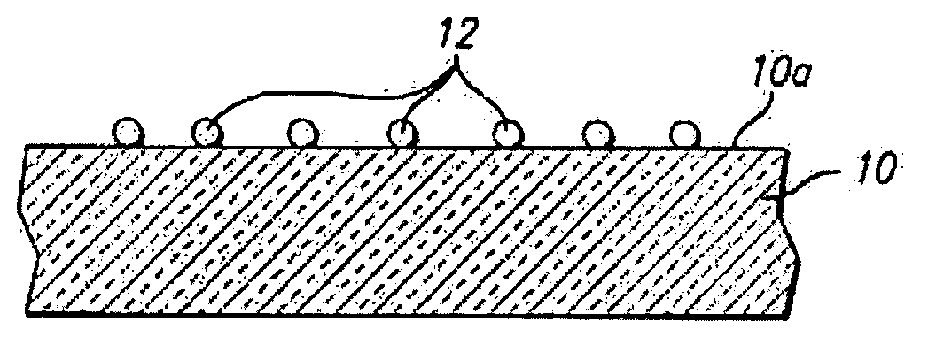
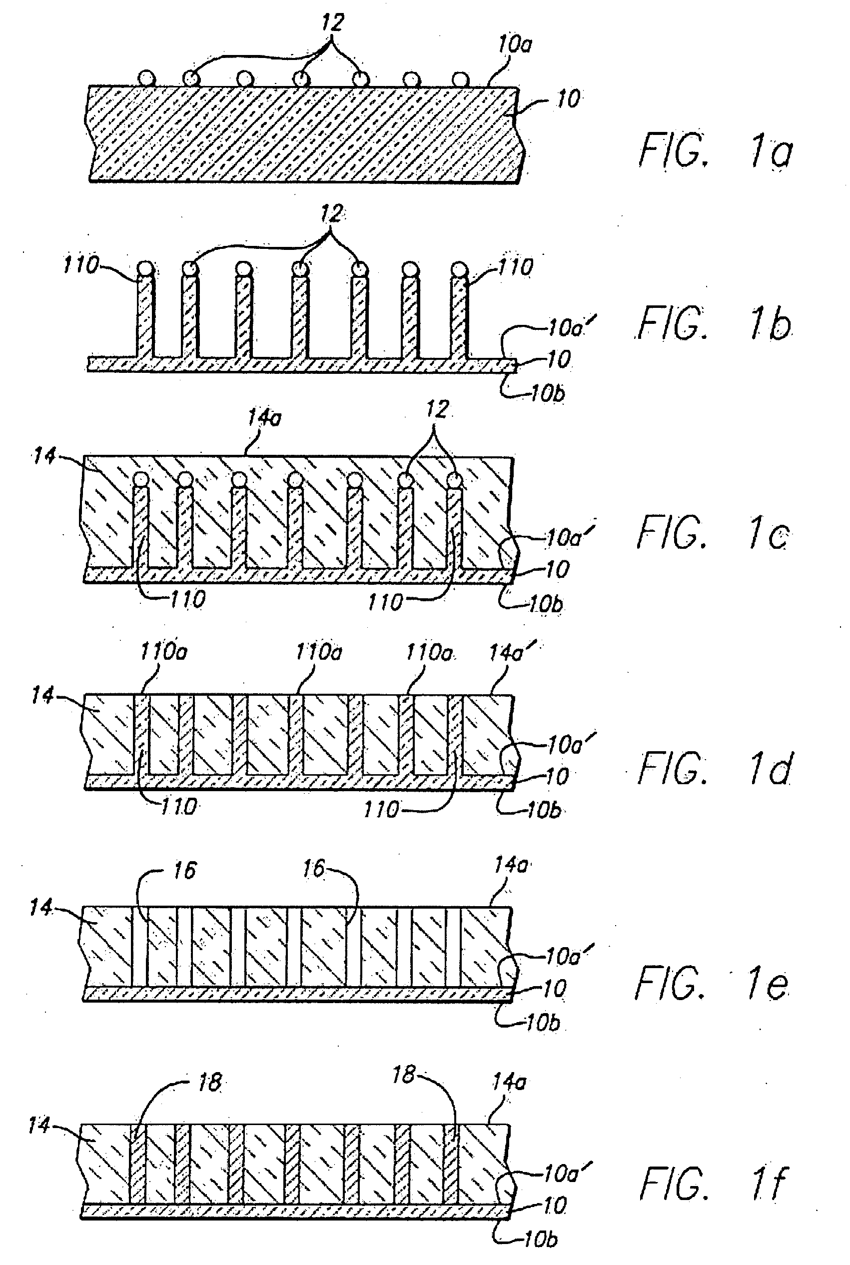
[0017]The discussion which follows is primarily directed to forming an array of nanopores. However, it will be appreciated that the same approach can be used to form a single nanopore.

[0018]In accordance with the present invention, a technique is provided for forming an array of molecules aligned in a pre-selected defined orientation relative to the substrate. In one embodiment, that orientation is preferably substantially perpendicular. The array of molecules is formed by dispersing them in an array of small, aligned holes (nanopores) in a substrate. Typically, the material in which the pores are formed is electrically insulating. The underlying substrate may be either electrically conducting or insulating. For electronic device applications, the substrate is generally electrically conducting and may be exposed and accessible at the bottom of the pores so that one end of the molecule in the nanopore makes electrical contact to the substrate. A substrate such as a single-crystal sil...


PUM

PropertyMeasurementUnit
particle sizeaaaaaaaaaa
diameteraaaaaaaaaa
lengthaaaaaaaaaa

Abstract

A technique is provided for forming a molecule or an array of molecules having a defined orientation relative to the substrate or for forming a mold for deposition of a material therein. The array of molecules is formed by dispersing them in an array of small, aligned holes (nanopores), or mold, in a substrate. Typically, the material in which the nanopores are formed is insulating. The underlying substrate may be either conducting or insulating. For electronic device applications, the substrate is, in general, electrically conducting and may be exposed at the bottom of the pores so that one end of the molecule in the nanopore makes electrical contact to the substrate. A substrate such as a single-crystal silicon wafer is especially convenient because many of the process steps to form the molecular array can use techniques well developed for semiconductor device and integrated-circuit fabrication.

Description

STATEMENT REGARDING FEDERALLY SPONSORED RESEARCH OR DEVELOPMENT[0001]The U.S. Government has a paid-up license in this invention and the right in limited circumstances to require the patent owner to license others on reasonable terms as provided for by the terms of Contract No. MDA 97201-3-0005 awarded by the Defense Advanced Research Projects Agency.TECHNICAL FIELD[0002]The present invention is related generally to forming nanopores useful for aligning molecules.BACKGROUND ART[0003]The field of molecular electronics relies on ordered placement of molecules on a supporting substrate, which is often an electrode of an electronic device. For most applications, the molecules should have a definite orientation or be oriented with respect to the substrate plane, often perpendicular to it. Molecular films are often formed by Langmuir-Blodgett techniques to obtain a uniform monolayer or multi-layer film. However, the orientation of the molecules is often difficult to control using Langmuir...

Claims


Application Information

Patent Timeline
Patent Type & Authority Applications(United States)
IPC IPC(8): B31D3/00H01L29/06C03C15/00C03C17/00H01L21/033H01L21/311
CPCB81C1/00031B82Y10/00C03C15/00H01L21/31144H01L21/0332H01L21/0337C03C17/001
Inventor KAMINS, THEODORE I.CHEN, YONGBECK, PATRICIA A.
Owner HEWLETT PACKARD DEV CO LP
Why Eureka
Try Eureka