Organic field effect tube using single molecular layer as oriented transfer layer and its preparing method

A technology of effect tube and organic field, which is applied in semiconductor/solid-state device manufacturing, electrical components, electric solid-state devices, etc., and can solve problems such as inconspicuous orientation effect, inconspicuous effect, and weak optical orientation effect

Inactive Publication Date: 2005-10-19
FUDAN UNIV
View PDF0 Cites 8 Cited by
  • Summary
  • Abstract
  • Description
  • Claims
  • Application Information

AI Technical Summary

Problems solved by technology

At the same time, some researchers also used the L-B monolayer technology to form an ordered film formation of the organic layer [8,9]. However, the orientation effect of the OFET device prepared by this method is not obvious, so the performance of the device is not greatly improved.
[0003] Although there has been a lot of research on orientation means and orientation technology, its effect is not obvious.
Although rubbing orientation has the best orientation effect, since the current research is all contact rubbing against the insulating layer or organic layer, it may cause dust pollution and static electricity, which will affect the yield of the device, because the deposition of the insulating layer Or organic layer devices can no longer be cleaned as thoroughly as ITO glass substrates
Although photo-orientation is a non-contact orientation method, its orientation effect depends on the intensity of ultraviolet light and the matching degree of ultraviolet light and insulating layer materials, and current studies have shown that the effect of photo-orientation is significantly weaker than that of rubbing orientation; L-B single molecule Layer-by-layer film formation technology is a film-forming method with simple film formation and orderly molecular arrangement, but the anisotropic effect of its film formation is far lower than that of rubbing orientation and photo-orientation, and the device performance needs to be improved.

Method used


Image

  • Organic field effect tube using single molecular layer as oriented transfer layer and its preparing method
  • Organic field effect tube using single molecular layer as oriented transfer layer and its preparing method

Examples


Embodiment 1

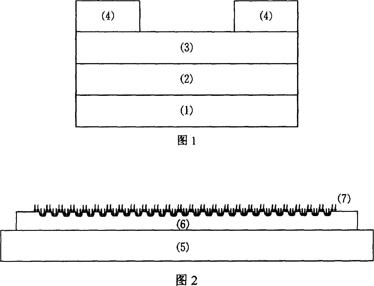
[0030] 1. First, clean the PET substrate with gate structure ITO after photolithography molding. The cleaning process is as follows: use special cleaning agent (10min), deionized water (3×10min), 50:8 isopropanol and Concentrated ammonia water mixed solution (10min), chloroform (10min), acetone (10min), and ethanol (10min) were subjected to ultrasonic treatment (treatment time in brackets), then fumigated with ethanol steam for 3 minutes, and finally UV treatment for 5 minutes;

[0031] 2. Secondly, anisotropic treatment of ITO was performed by mechanical friction. The friction material used is YA-18-R rayon flannelette provided by Yoshikawa Chemical Co. The average length of the rayon front of the flannelette is 600 μm, the average diameter is 15 μm, and the fiber density is 3200 thread / cm 2 . During mechanical friction, the drum rotates at 1500 rpm, and after 10 times of friction treatment, clean it with deionized water;

[0032] 3. Use 40g / mol concentration of NaOH soluti...

Embodiment 2

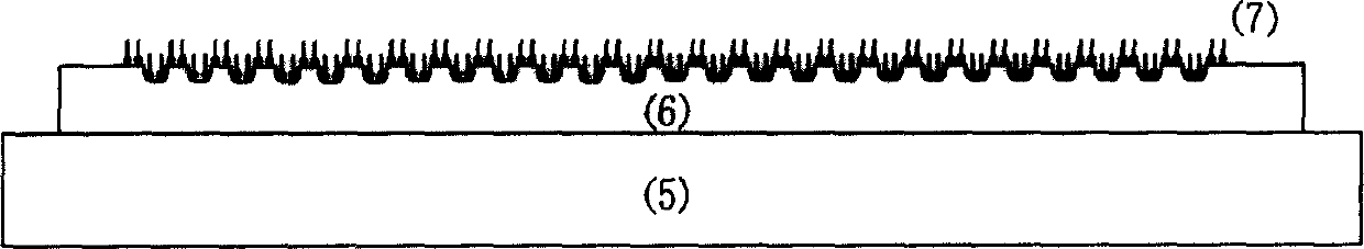
[0035] 1. First, clean the glass substrate with gate structure ITO after photolithography molding. The cleaning process is as follows: use special cleaning agent (10min), deionized water (3×10min), 50:8 isopropanol and Concentrated ammonia water mixed solution (10min), chloroform (10min), acetone (10min), and ethanol (10min) were subjected to ultrasonic treatment (treatment time in brackets), then fumigated with ethanol steam for 3 minutes, and finally UV treatment for 5 minutes;

[0036] 2. Secondly, stripes are carved on the surface of ITO by means of photolithography or laser etching to form anisotropy;

[0037] 3. Use 30g / mol concentration of NaOH solution to clean the surface of the ITO substrate for about 1 minute; then use chromic acid in chloroform solution (concentration of about 30%) to soak or ultrasonic for about 8 seconds for surface treatment; then use vinyl triethoxy Treat the surface of the substrate with base silane to form a monomolecular film;

[0038] 4. T...


PUM


Abstract

This invention provides an OFET device and its preparation method including an orientation transfer layer for transferring orientation efficiency, which can increase the carrier mobility of the OFET since the orientation transfer layer is the insulation one. Said one is a mono-film formed by processing the surface with silane coupler which can optimize the orientation result of the orientation layer and transfer it to the organic layer. This invention can improve molecular arrays of the organic molecular layer by transferring the orientation result to improve the carrier mobility of the OFET devices applying said orientation layer.

Description

technical field [0001] The invention belongs to the technical field of organic field effect tubes (OFETs), and in particular relates to an organic field effect tube using a monomolecular layer as an orientation transfer layer and a preparation method thereof. technical background [0002] The field effect transistor is a semiconductor device that uses the magnitude of the gate voltage to adjust the carrier density between the source and drain electrodes, thereby controlling the on-off of the channel current and forming a switching characteristic. Organic Field Effect Transistor (OFET) is a semiconductor device that uses organic materials as insulating layer and semiconductor layer, and its basic principle is basically the same as that of non-field effect transistor devices. However, compared with field effect tubes without field effects, it has the advantages of simple process, low cost, and can be made into flexible devices. After more than ten years of research, the perfo...

Claims


Application Information

Patent Timeline
Patent Type & Authority Applications(China)
IPC IPC(8): H01L51/40
Inventor 黄维张天翼许军钱东金白春礼
Owner FUDAN UNIV
Why Eureka
Try Eureka