Display device
- Summary
- Abstract
- Description
- Claims
- Application Information
AI Technical Summary
Benefits of technology
Problems solved by technology
Method used
Image

Examples
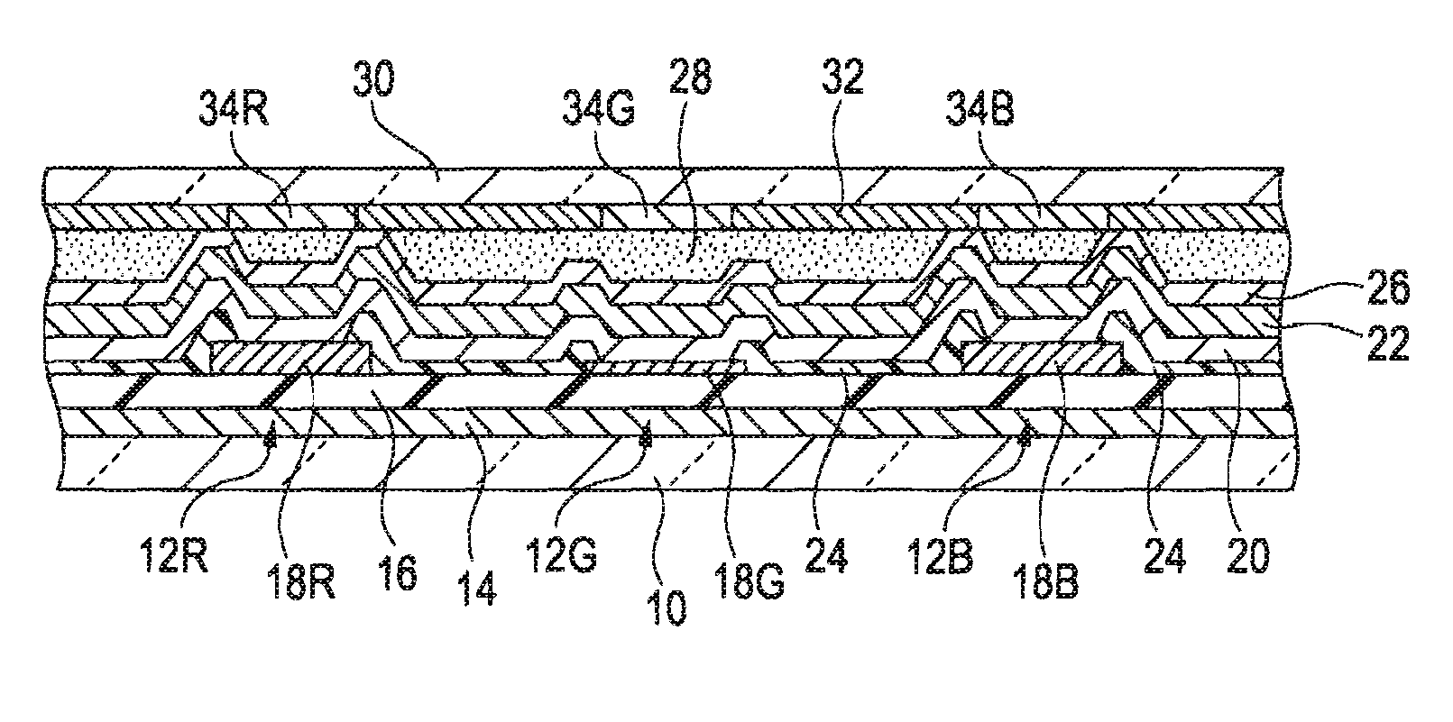
first embodiment
Modification of First Embodiment
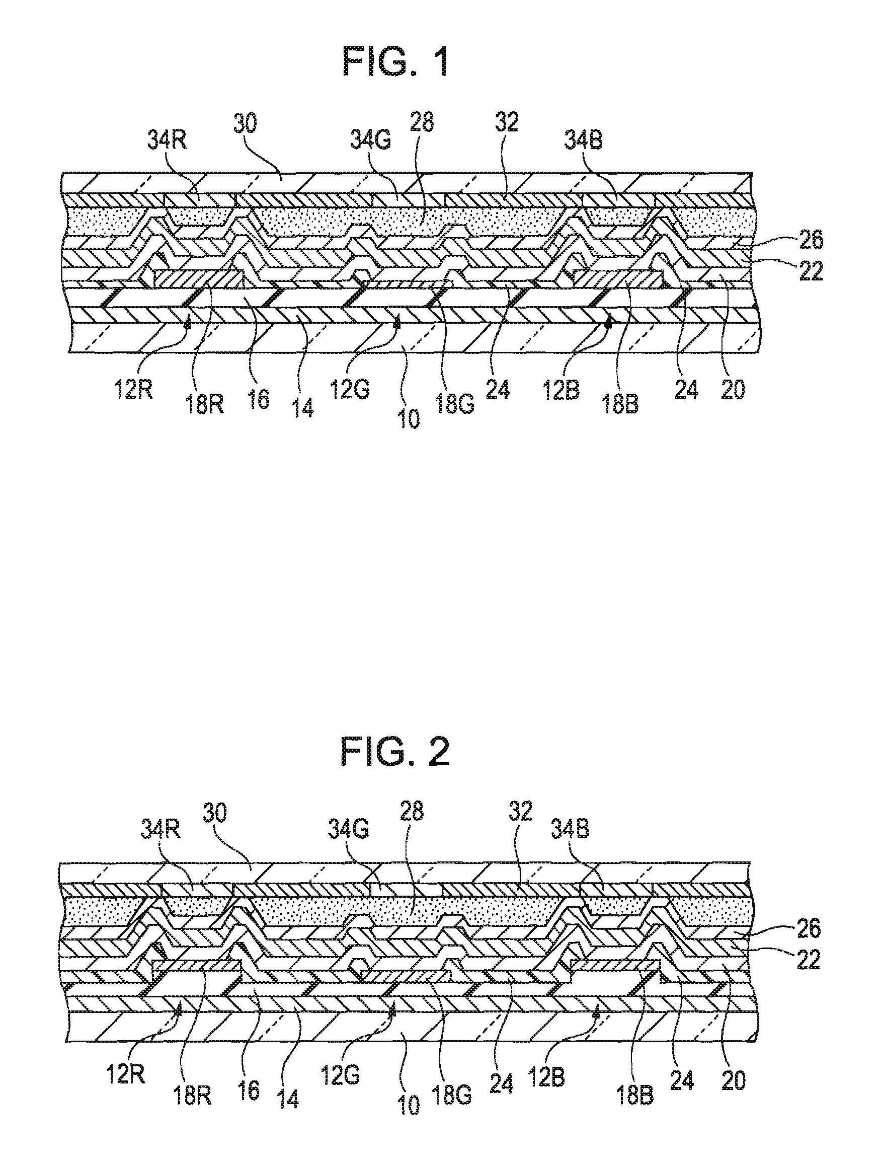
[0056]FIG. 2 is a cross-sectional view of a full-color display device of the top emission type according to a modification of the first embodiment of the invention. In FIG. 2, the same reference numbers are used or components common to those in the first embodiment, and the descriptions thereof are omitted.
[0057]In this modification, the pixel electrode layers 18R, 18G, and 18B in the light-emitting elements 12R, 12G, and 12B, respectively, are composed of the same material and have the same thickness. The material of the insulating transparent layer 16 is the same at each of the light-emitting elements 12R, 12G, and 12B, and the thickness of the insulating transparent layer 16 is the same at the light-emitting elements 12R and 12B. However, the thickness of the insulating transparent layer 16 at the light-emitting elements 12G differs from those of the insulating transparent layer 16 at the light-emitting elements 12R and 12B.
[0058]Since the material...
first example of first embodiment
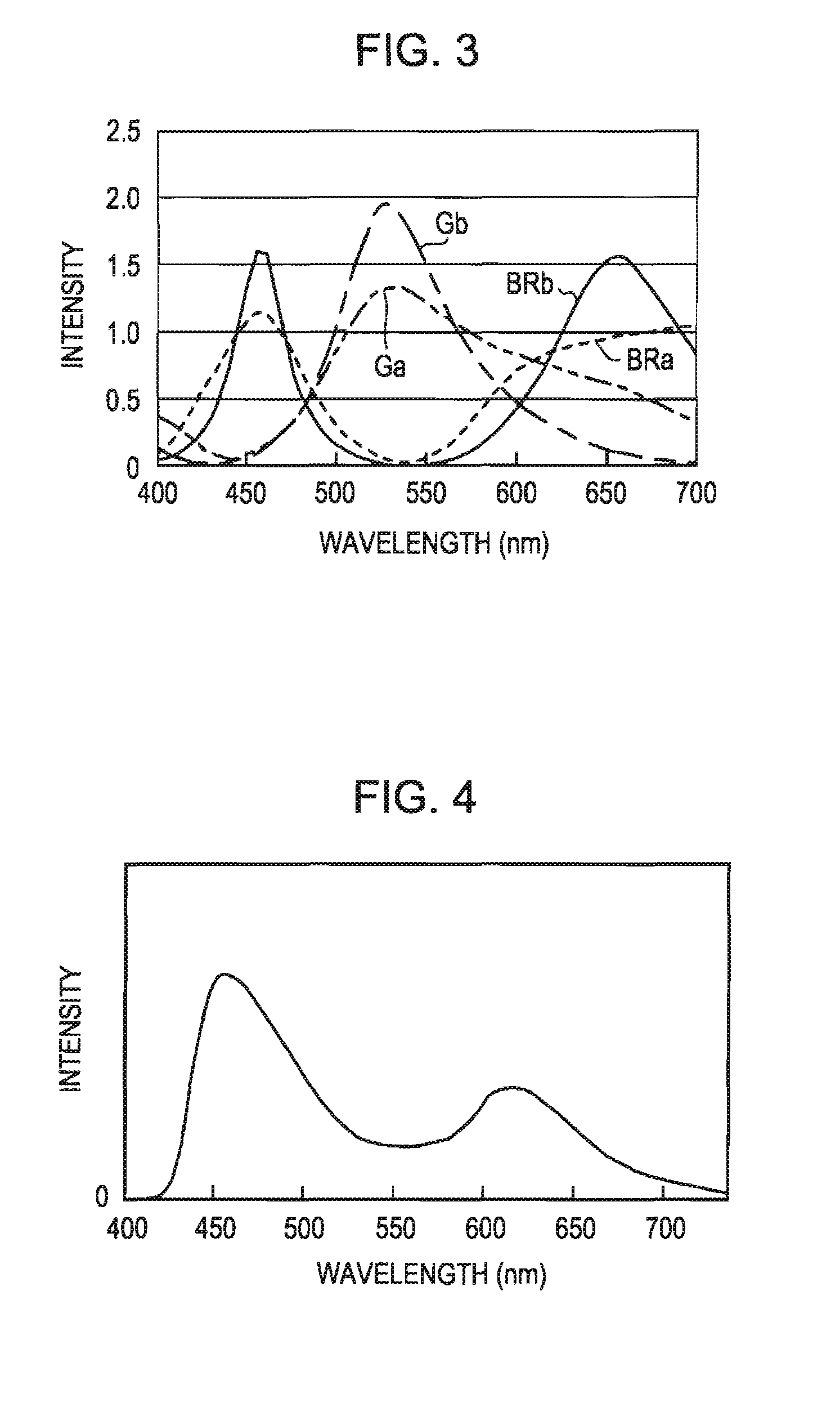
[0060]Optical characteristics of the display device having the structure according to the first embodiment shown in FIG. 1 were investigated by simulation.
[0061]The simulation was performed under the following conditions. The insulating transparent layer 16 was composed of silicon nitride and had a uniform thickness of 50 nm. The pixel electrode layers 18G in the light-emitting elements 12G were composed of ITO and had a thickness of 60 nm. The electrode layers 18R and 18B in the light-emitting elements 12R and 12B, respectively, were composed of ITO and had a thickness of 130 nm. The counter electrode layer 22 was made transparent (hereinafter, a case including a transparent counter electrode layer 22 is referred to as an example of a layer without a half mirror).
[0062]In another example, a display device was formed under the same conditions as above except that the second sublayer of the counter electrode layer 22 was composed of an alloy of magnesium and silver so as to form a tr...
second example of first embodiment
[0072]The spectra of light passing through the protective layer 26 and the spectra of light passing through the color filters 34 were investigated by simulation using the light-emitting sublayer exhibiting the emission spectrum shown in FIG. 6. As shown in FIG. 6, the light-emitting sublayer is an existing white-light emitting layer having three intensity peaks at wavelengths corresponding to blue, green, and red.
[0073]FIG. 7 illustrates simulation results of the spectra of light passing through the protective layer 26 and the spectra of light passing through the color filters 34 using the light-emitting sublayer exhibiting the emission spectrum shown in FIG. 6 in the first embodiment. FIG. 7 shows results of the example in which the counter electrode layer 22 was transparent, and did not include the half mirror.
[0074]The simulation was performed under the following conditions. The insulating transparent layer 16 was composed of silicon nitride and had a uniform thickness of 50 nm. ...
PUM
| Property | Measurement | Unit |
|---|---|---|
| Length | aaaaa | aaaaa |
| Thickness | aaaaa | aaaaa |
| Transparency | aaaaa | aaaaa |
Abstract
Description
Claims
Application Information
 - Generate Ideas
- Intellectual Property
- Life Sciences
- Materials
- Tech Scout
- Unparalleled Data Quality
- Higher Quality Content
- 60% Fewer Hallucinations
Browse by: Latest US Patents, China's latest patents, Technical Efficacy Thesaurus, Application Domain, Technology Topic, Popular Technical Reports.
© 2025 PatSnap. All rights reserved.Legal|Privacy policy|Modern Slavery Act Transparency Statement|Sitemap|About US| Contact US: help@patsnap.com