Compact dual-band resonator using anisotropic metamaterial
- Summary
- Abstract
- Description
- Claims
- Application Information
AI Technical Summary
Benefits of technology
Problems solved by technology
Method used
Image
Examples
example
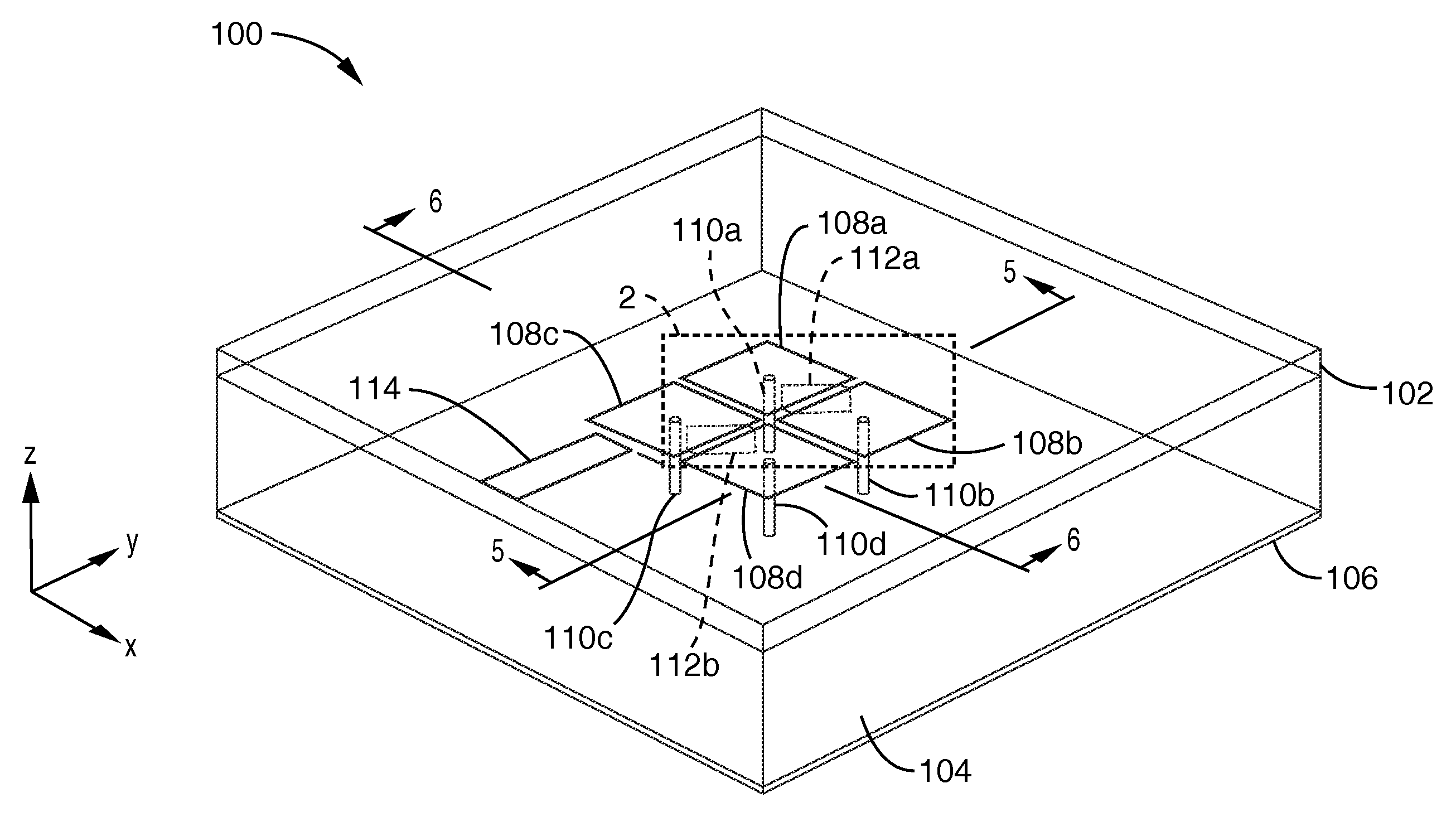
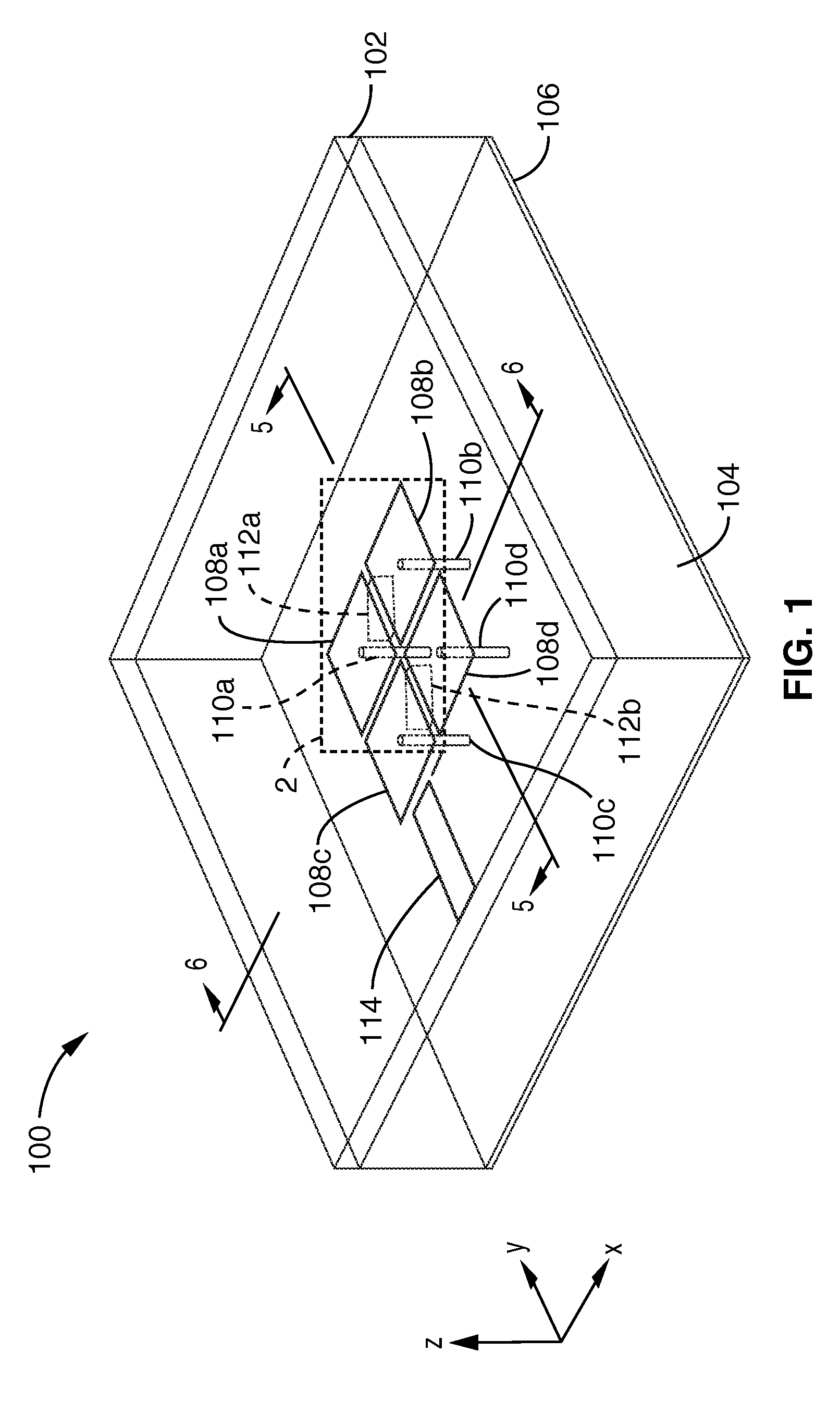
[0046]A prototype compact dual-band antenna was fabricated using the design shown in FIG. 1 through FIG. 3 and FIG. 4 through FIG. 8 and the dimensions shown in FIG. 9 and FIG. 10 for operation generally at 1.9 GHz and 2.4 GHz in the x- and y-directions, respectively. RT / Duroid material was used for the substrate, and 0.8 mil thick copper was used for the patches. The thicknesses of the upper substrate layer was chosen so that its dielectric constant ∈ was much greater than that of the lower substrate layer, the dielectric constants of the upper and lower layers being approximately 10.0 and 2.2, respectively. The microstrip feedline was positioned in an offset feed configuration and coupled to the antenna by a 0.1 mm gap. The particular width of the microstrip feedline was chosen for impedance matching at 50-ohms.
[0047]As can be seen in the figures, the left edge of the feedline is offset from the left edge of the patch by 0.4 mm. This places the center of the feedline at 0.325 mm l...
PUM
 Abstract
Description
Claims
Application Information


