Exposure method and exposure apparatus, and device manufacturing method

Inactive Publication Date: 2008-08-28
NIKON CORP
View PDF25 Cites 51 Cited by
  • Summary
  • Abstract
  • Description
  • Claims
  • Application Information

AI Technical Summary

Benefits of technology

[0033]Further, in a lithography process, by using any one of the exposure methods in the first to fifth exposure methods of the present invention to form a device pattern on an object, the device pattern can be formed on the object with good precision. Accordingly, it can also be said from another aspect that the present invention is a device manufacturing method including a lithography process that uses any one of the exposure methods in the first to fifth exposure methods of the present invention to form a device pattern on an object. S

Problems solved by technology

Therefore, in a dioptric system consisting only of lenses, it becomes difficult to satisfy the Petzval condition, which tends to lead to an increase in the size of the projection optical system.
However, the aberration change as is shown in the contour line drawing in FIG. 16B is difficult to correct by the image-forming characteristics correction mechanism typically employed in an exposure apparatus, such as the mechanism of vertically moving, or tilting the lenses that constitute a part of the pro

Method used


Image

  • Exposure method and exposure apparatus, and device manufacturing method
  • Exposure method and exposure apparatus, and device manufacturing method
  • Exposure method and exposure apparatus, and device manufacturing method

Examples


Embodiment Construction

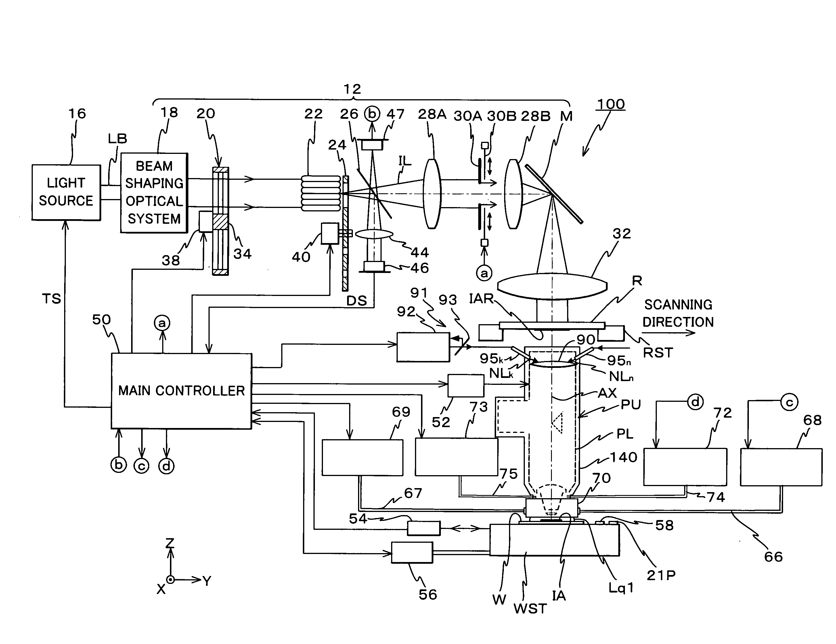
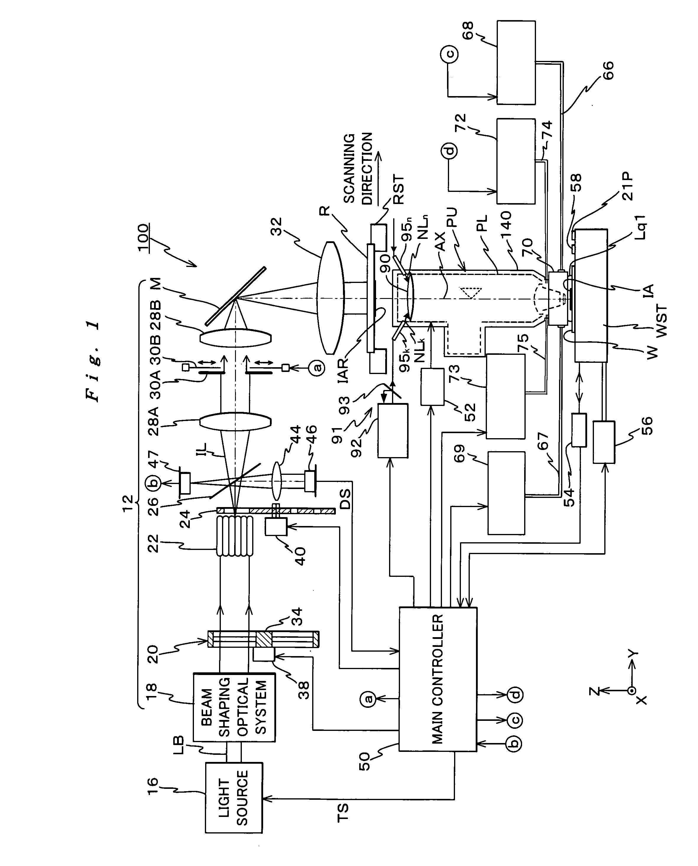
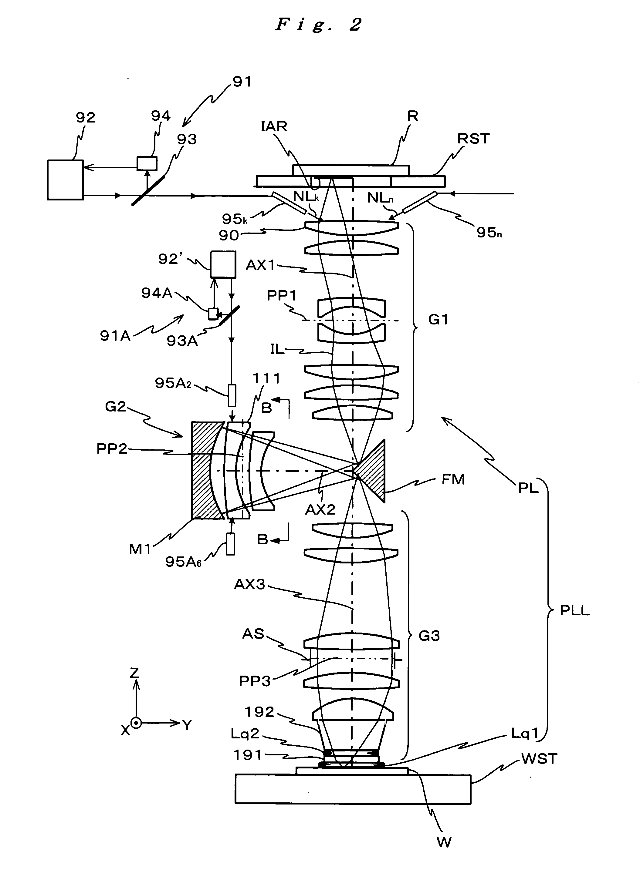
[0051]An embodiment of the present invention is described below, referring to FIGS. 1 to 13.

[0052]FIG. 1 schematically shows an arrangement of an exposure apparatus 100 related to an embodiment. Exposure apparatus 100 is a scanning exposure apparatus by the step-and-scan method, that is, the so-called scanner.

[0053]Exposure apparatus 100 is equipped with the following: an illumination system that includes a light source 16 and an illumination optical system 12; a reticle stage RST that holds a reticle R, which is illuminated by an exposure illumination light IL emitted from the illumination system, and moves in a predetermined scanning direction (in this case, a Y-axis direction, which is the lateral direction within the page surface of FIG. 1); a projection unit PU that includes a projection optical system PL, which projects the pattern of reticle R on a wafer W serving as an object; and a wafer stage WST that holds wafer W and moves on a horizontal surface (within an XY plane), an...


PUM


Abstract

By the combination of adjusting optical properties of an optical system by an irradiation unit irradiating non-exposure light on an optical element, which is movable, and adjusting the optical properties of the optical system with an optical properties adjustment unit by moving the optical element, for example, the change in the optical properties of the optical system caused by the temperature distribution of the optical elements whose center is at a position eccentric from the optical axis is corrected. Further, under a dipole illumination condition, in order to make optical properties of an optical system caused by non-rotational symmetry temperature distribution of optical elements in the vicinity of pupils into optical properties that can be corrected more easily by an optical properties adjustment unit, an irradiation unit irradiates non-exposure light on an optical element, which makes the optical element have a rotational symmetry temperature distribution. Accordingly, optical properties change in the optical system due to illumination light absorption can be effectively corrected.

Description

CROSS-REFERENCE TO RELATED APPLICATIONS[0001]This non-provisional application claims the benefit of Provisional Application No. 60 / 734,759 filed Nov. 9, 2005, the disclosure of which is hereby incorporated herein by reference in its entirety.BACKGROUND OF THE INVENTION[0002]1. Field of the Invention[0003]The present invention relates to exposure methods and exposure apparatus, and device manufacturing methods, and more particularly to an exposure method and an exposure apparatus that are used in a lithography process in which electronic devices such as a semiconductor device (an integrated circuit) or a liquid crystal display device are manufactured, and a device manufacturing method that uses the exposure method and the exposure apparatus.[0004]2. Description of the Related Art[0005]Conventionally, in a lithography process for manufacturing electronic devices (microdevices) such as a semiconductor device (an integrated circuit or the like), a liquid crystal display device, or the l...

Claims


Application Information

Patent Timeline
IPC IPC(8): G03B27/42
CPCG03F7/70891G03F7/70258G03F7/70308
Inventor UEHARA, YUSAKUUCHIKAWA, KIYOSHIISHIYAMA, SATOSHI
Owner NIKON CORP
Why Eureka
Try Eureka