Method for fault handling in a converter circuit for wiring of three voltage levels

a fault handling and voltage level technology, applied in the field of converter circuits, can solve the problems of destroying the igbt, putting a burden on the power semiconductor switch, and extreme power loss, and achieve the effect of less burden, avoiding damage to the power semiconductor switch, and reducing the risk of failur

Active Publication Date: 2008-08-28
ABB (SCHWEIZ) AG
View PDF8 Cites 17 Cited by
  • Summary
  • Abstract
  • Description
  • Claims
  • Application Information

AI Technical Summary

Benefits of technology

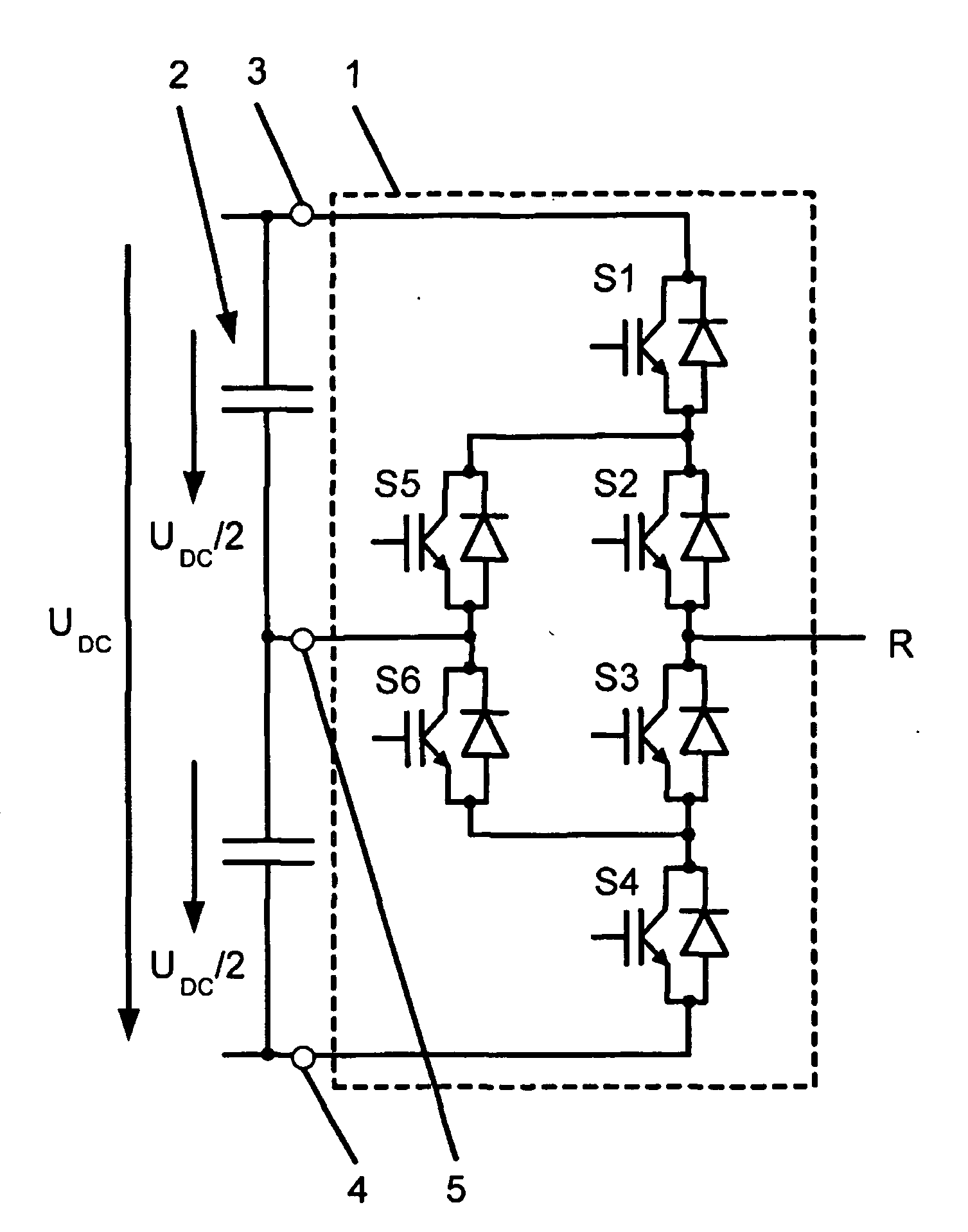
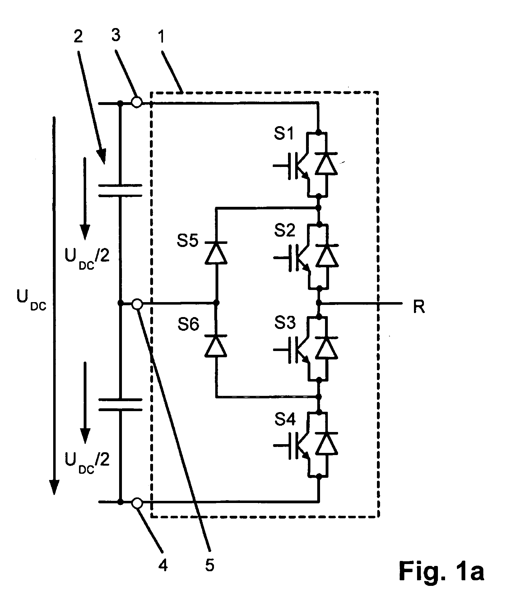
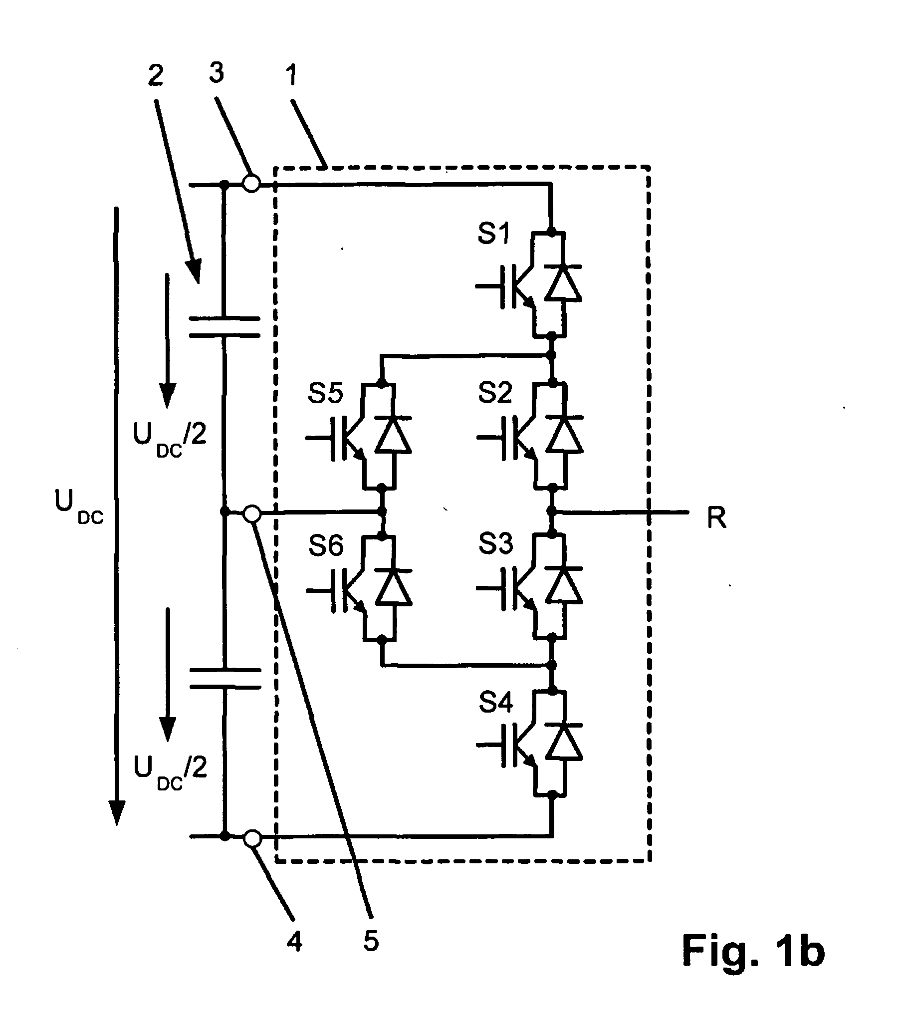
[0009]One exemplary method for fault handling in a converter circuit for switching three voltage levels, the converter circuit has a converter subsystem provided for each phase and comprises a DC voltage circuit formed by two series-connected capacitors, where the DC voltage circuit comprises a first principal connection and a second principal connection and a subconnection formed by the two adjacent and interconnected capacitors. In addition, each converter subsystem has a first, a second, a third and a fourth actuatable bidirectional power semiconductor switch and a fifth and a sixth power semiconductor switch, the first, second, third and fourth power semiconductor switches being connected in series. The first power semiconductor switch is connected to the first principal connection and the fourth power semiconductor switch is connected to the second principal connection. In addition, the fifth and sixth power semiconductor switches are connected in series, the junction between the fifth power semiconductor switch and the sixth power semiconductor switch being connected to the subconnection, the fifth power semiconductor switch being connected to the junction between the first power semiconductor switch and the second power semiconductor switch, and the sixth power semiconductor switch being connected to the junction between the third power semiconductor switch and the fourth power semiconductor switch. The method additionally involves detection of a top fault current path or a bottom fault current path in the converter subsystem when a fault occurs in the converter subsystem, the top fault current path running through the first, second, third and sixth power semiconductor switches or through the first and fifth power semiconductor switches, and the bottom fault current path running through the second, third, fourth and fifth power semiconductor switches or through the fourth and sixth power semiconductor switches. In addition, the power semiconductor switches are switched on the basis of a fault switching sequence. The fault switching sequence in the event of detection of the top or bottom fault current path is followed by the detection's accompanying switching status of each actuatable bidirectional power semiconductor switch being recorded. The effect advantageously achieved by this is that there is first of all no further actuation of the actuatable bidirectional power semiconductor switches and hence also no switching action. In the event of detection of the top fault current path in the converted section system, the first power semiconductor switch and then the third power semiconductor in the converted section system can be turned off. In the event of detection of the bottom fault current path in the converted section system, the fourth power semiconductor switch and then the second power semiconductor switch in the converted section system can be turned off. Advantageously, the effect which may be achieved by this is that the converted section system affected by the fault and hence the entire converter circuit is put into a safe operating state. The power semiconductor switches in the converter circuit's converter systems which are not affected by the fault can be turned off. This allows formation of a short circuit current in the converter subsystem affected by the fault and any other converted section systems to be largely avoided, which means that the power semiconductor switches in the converter subsystem affected by the fault and also those in the other converter subsystems are subjected to less of the burden. The ageing of the power semiconductor switches can therefore advantageously be slowed down and damage to the power semiconductor switches can be largely prevented. Overall, this increases the availability of the converter circuit.
[0010]In one aspect, turning off the relevant two power semiconductor switches upon detection of a top or bottom fault current path advantageously produces a freewheeling path for the load current flowing in normal operation of the converter circuit, the DC voltage circuit also advantageously being protected against a short as a result of the relevant two power semiconductor switches being turned off.

Problems solved by technology

Secondly, a high anode / cathode voltage is simultaneously applied between the anode and the cathode of the IGBT.
This results in an extremely high instantaneous power loss which can destroy the IGBT.
The short on all phases of the converter circuit from DE 699 02 227 T2 allows a short circuit current to be produced in the converter subsystem affected by the fault and in the other converter subsystems, however, said short circuit current placing a burden on the power semiconductor switches.
A power semiconductor switch burdened in this manner can therefore age more quickly or can even be damaged, which means that the availability of the converter circuit is severely impaired or at worst is eliminated.

Method used


Image

  • Method for fault handling in a converter circuit for wiring of three voltage levels
  • Method for fault handling in a converter circuit for wiring of three voltage levels
  • Method for fault handling in a converter circuit for wiring of three voltage levels

Examples


Embodiment Construction

[0021]FIG. 1a shows the exemplary converter subsystem 1 in a converter circuit for switching three voltage levels. The converter circuit has a converter subsystem 1 provided for each phase R, S, T, FIG. 1a showing just one converter subsystem 1 for the phase R. The converter circuit comprises a DC voltage circuit 2 formed by two series-connected capacitors, the DC voltage circuit 2 having a first principle connection 3 and a second principle connection 4 and a subconnection 5 formed by the two adjacent and interconnected capacitors. In addition, the converter subsystem 1 has a first, a second, a third and a fourth actuatable bi directional power semiconductor switch S1, S2, S3, S4 and a fifth and a sixth power semiconductor switch S5, S6. The respective actuable bidirectional power semiconductor switch S1, S2, S3, S4 is, in particular, formed by an insulated gate bipolar transistor (IGBT) and by a diode connected back-to-back with the bipolar transistor. However, it is also conceiva...


PUM


Abstract

The document specifies a method for fault handling in a converter circuit for switching three voltage levels, in which the converter circuit has a converter subsystem provided for each phase (R,S,T), in which a top fault current path (A) or a bottom fault current path (B) in the converter subsystem is detected, the top fault current path (A) running through the first, second, third and sixth power semiconductor switches in the converter subsystem or through the first and fifth power semiconductor switches (S1, S5) in the converter subsystem, and the bottom fault current path (B) running through the second, third, fourth and fifth power semiconductor switches in the converter subsystem or through the fourth and sixth power semiconductor switches in the converter subsystem, and in which the power semiconductor switches are switched on the basis of a fault switching sequence. To avoid phase shorting of all the phases of the converter circuit in order to achieve a safe operating state for the converter circuit in the event of a fault, the fault switching sequence in the event of detection of the top or the bottom fault current path (A, B) is initially followed by the detection's accompanying switching status of each power semiconductor switch being recorded. In addition, in the event of detection of the top fault current path (A) the first power semiconductor switch and then the third power semiconductor are turned off, and in the event of detection of the bottom fault current path (B) the fourth power semiconductor switch and then the second power semiconductor are turned off.

Description

CROSS REFERENCE TO RELATED APPLICATIONS[0001]This application claims priority under 35 U.S.C. §119 to EP Application 04405373.4 filed in Europe on 18 Jun. 2004, and as a continuation application under 35 U.S.C. §120 to PCT / CH2005 / 000203 filed as an International Application on 11 Apr. 2005 designating the U.S., the entire contents of which are hereby incorporated by reference in their entireties.FIELD[0002]Actuation methods for converter circuits are disclosed. Specifically, a method for fault handling in a converter circuit for switching three voltage levels is disclosed.BACKGROUND INFORMATION[0003]Power semiconductor switches are currently being used increasingly in converter technology and particularly in converter circuits for switching three voltage levels. Such a converter circuit for switching three voltage levels is specified in DE 699 02 227 T2. FIG. 1a shows a converter subsystem for a phase of the converter circuit, where the converter subsystem shown in FIG. 1a correspon...

Claims


Application Information

Patent Timeline
Patent Type & Authority Applications(United States)
IPC IPC(8): H02H9/02H02H3/08B60L3/00H02H7/122H02P27/14
CPCH02H7/1225H02M7/487H02M1/32H02M7/48
Inventor KNAPP, GEROLDHOCHSTUHL, GERHARDWIESER, RUDOLFMEYSENC, LUC
Owner ABB (SCHWEIZ) AG
Why Eureka
Try Eureka