
Method and Device for In-Band Optical Performance Monitoring

a technology of optical performance monitoring and in-band measurement, applied in the direction of transmission monitoring, electrical equipment, electromagnetic transmission, etc., can solve the problems of osa method failing in reconfigurable networks, reducing the resolution bandwidth of osa will be of no benefit, and osa method failing in wdm systems with high spectral efficiency

Inactive Publication Date: 2008-08-28
NICTA IPR
View PDF22 Cites 42 Cited by
  • Summary
  • Abstract
  • Description
  • Claims
  • Application Information

AI Technical Summary

Benefits of technology

[0029]Further, by separately converting the first and second optical signal components into the electrical domain, the present invention enables greater application of electrical signal processing techniques. Exploitation of such electrical signal processing techniques can reduce the performance requirements on devices used to process the optical signal components, thus allowing prospective implementation with low cost optical components. For example, no polarisation control is required in some embodiments of the invention.
[0030]In some embodiments of the invention the electrical bandwidth of the photodetectors may be substantially less than the signal bandwidth. Since the ASE beat noise is approximately constant across the spectrum, the low frequency components can be used to determine the OSNR. If both receivers have identical response functions the distorted signals induced by the low bandwidth filtering will be common to both channels and can therefore be cancelled. As well as reducing the cost, the low speed embodiment is less sensitive to timing offsets and to 1st order PMD.
[0034]In further embodiments of the invention, equalising of the signal power of the first electrical signal component and the signal power of the second electrical signal component may comprise monitoring the signal power of the first and second electrical signal components, and by waiting for polarisation changes in the optical signal to cause equalisation from time to time. In some such embodiments, the optical signal may be passed through a rotating quarter wave plate prior to splitting in order to increase the regularity with which polarisation changes cause equalisation.
[0043]Preferably, the first optical signal component and the second optical signal component undergo substantially equal delay prior to conversion to the electrical domain, such that the output of the subtractive combination of the first electrical signal and the second electrical signal is substantially noise only across the whole band. For example, upon splitting, the first optical signal component and the second optical signal component may each be passed directly to respective photodetectors for conversion to the electrical domain, thus ensuring equal delay. Such embodiments are particularly advantageous as noise may be directly measured in-band and across the entire band of interest.

Problems solved by technology

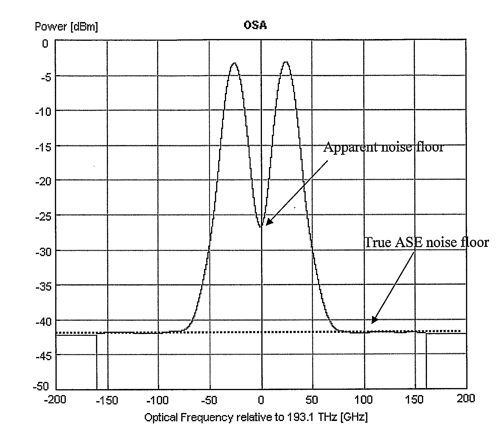
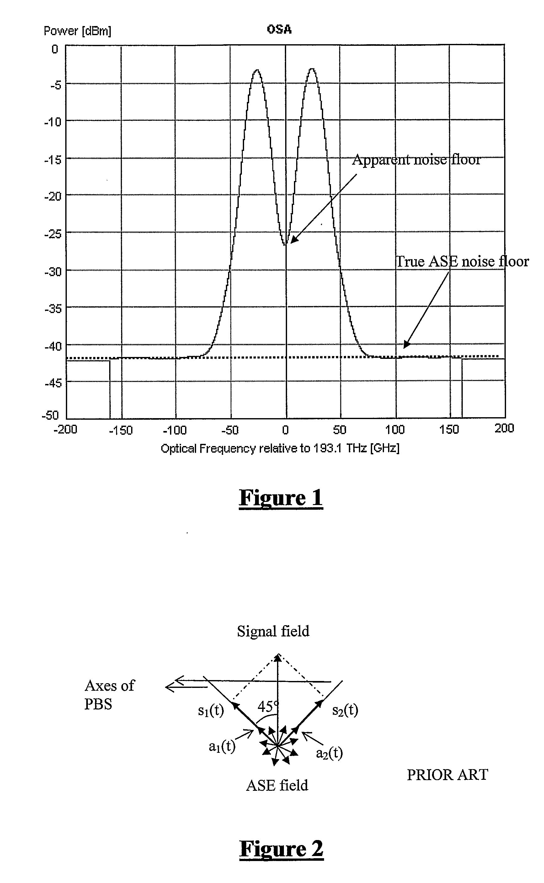
However, the OSA method fails for WDM systems with high spectral efficiency, as shown in FIG. 1, in which the optical spectrum of 10 GB / s NRZ signals with 50 GHz spacing (0.1 nm resolution) is illustrated.
Notably, the modulation sidebands between such closely spaced channels mask the true OSNR level, and reduction of the resolution bandwidth of the OSA will be of no benefit.
The OSA method also fails in reconfigurable networks where different channels may traverse through different optical paths.
While a simple concept, this method has difficulty in distinguishing various sources of noise impairment, and further requires a high speed detector.
However, this method is dependent on signal format and bit rate, and can only measure RF noise at half bit rate for RZ signals.
Further, this method assumes that noise measured at the half bit rate is indicative of noise across signal bandwidth, and assumes that noise sources are isotropic in phase space.
However in this case, the relative delay in the polarisation states is obtained by introducing a polarisation maintaining (PM) fiber with a large DGD in place of the PMD emulator.

Method used


Image

  • Method and Device for In-Band Optical Performance Monitoring
  • Method and Device for In-Band Optical Performance Monitoring
  • Method and Device for In-Band Optical Performance Monitoring

Examples


first embodiment

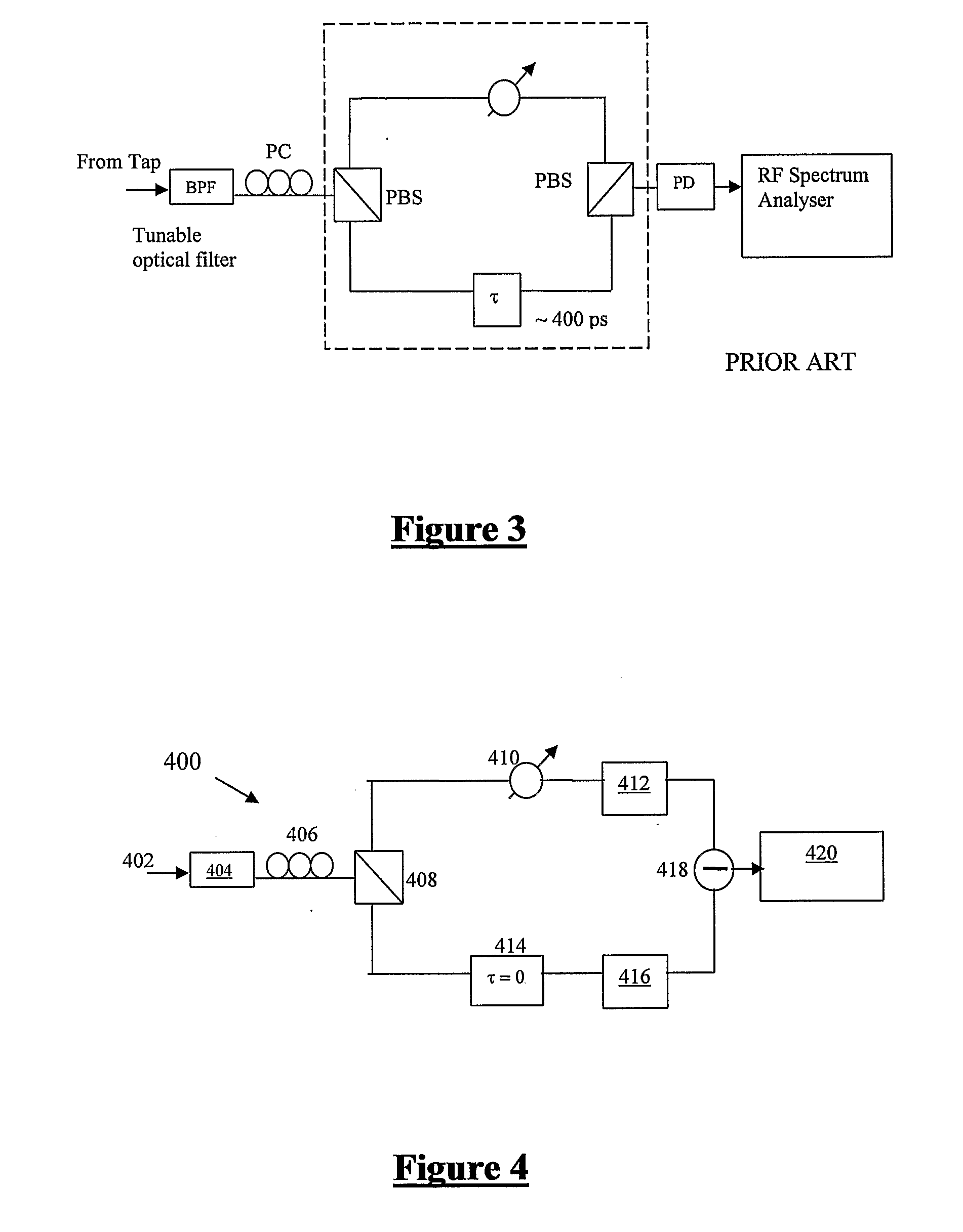
[0061]FIG. 4 is a schematic of an OSNR monitoring device 400 in accordance with the present invention. An input optical signal 402 is tapped from a WDM optical network being monitored. The input optical signal 402 is first passed through a tunable optical bandpass filter 404 to ensure only a band of interest is processed. From filter 404, the optical signal is passed through a polarisation controller 406 to orient the polarised data signal at 45 degrees to the input of a polarisation beam splitter 408. Polarisation beam splitter 408 splits the optical signal to produce a first optical signal component and a second optical signal component, which will each carry a substantially equal signal power due to the 45 degree polarisation applied by polarisation controller 406.

[0062]The first optical signal component is passed through a variable optical attenuator 410, and then converted to the electrical domain by photodetector 412 to produce a first electrical signal component. The second o...

second embodiment

[0067]In embodiments of the invention in which cost reduction in respect of the polarisation beam splitter is sought, a low cost polarisation beam splitter with poor extinction ratio (perhaps as low as 3 dB) could be used. Alternatively, FIG. 5 illustrates an OSNR monitoring device 500 in accordance with the present invention, in which the polarisation beam splitter is replaced with a 3 dB coupler, one arm of which is polarised. In considering FIG. 5 in more detail, an input optical signal 502 is tapped from a WDM optical network being monitored. The input optical signal 502 is first passed through a tunable optical bandpass filter 504 to ensure only a band of interest is processed. From filter 504, the optical signal is passed through a polarisation controller 506 to orient the polarised data signal at substantially 45 degrees to the axis of a polariser 512. Power splitter 508 splits the optical signal to produce a first optical signal component and a second optical signal componen...

third embodiment

[0070]It is noted that without polarisation controllers 406, 506 in FIGS. 4 and 5, signal cancellation and noise extraction could not occur at 418, 518 when the polarisation of the input signal 402, 502 is aligned with that of the PBS 408 or polariser 512. FIG. 6 is a schematic of an OSNR monitoring device 600 in accordance with the invention, which builds on the OSNR monitoring device of FIG. 5 by inclusion of a second polariser 632 at substantially 45° to the first polariser 612 to ensure that OSNR can be measured for all input polarisation states, without requiring a polarisation controller at the input. An input optical signal 602 is tapped from a WDM optical network being monitored. The input optical signal 602 is first passed through a tunable optical bandpass filter 604 to ensure only a band of interest is processed. From filter 604, the optical signal is passed to the input of a simple power splitter 608. Power splitter 608 splits the optical signal to produce a first optica...


PUM


Abstract

A method and device for determining in-band noise of an optical signal. The optical signal is split to produce two optical signal components, of distinct polarisation, such that the respective noise component in each signal component is uncorrelated. The optical signal components are converted to the electrical domain to produce electrical signal components. The signal component powers are equalised either in the optical domain or the electrical domain. The equalised electrical signal components are then subtracted together to cancel the correlated portions of the signal components (e.g. the data signal), such that only uncorrelated signal components (e.g. noise) are output for measurement.

Description

CROSS-REFERENCE TO RELATED APPLICATIONS[0001]The present application claims priority from Australian Provisional Patent Application No 2005902178 filed on 29 Apr. 2005, the content of which is incorporated herein by reference.TECHNICAL FIELD[0002]The present invention relates to measurement of a signal to noise ratio in an optical network, and in particular relates to in-band measurement of the signal to noise ratio.BACKGROUND ART[0003]In order to monitor the performance of wavelength division multiplexed (WDM) optical networks it is useful to have a measurement of the signal to noise ratio (SNR) of each wavelength channel at various points throughout the network. In networks that are predominantly degraded by amplified spontaneous emission (ASE) noise the SNR is correlated with the optical signal to noise ratio (OSNR).[0004]The OSNR has traditionally been measured with an optical spectrum analyser (OSA). The in-band OSNR can be estimated by interpolating ASE noise floor measured at...

Claims


Application Information

Patent Timeline
IPC IPC(8): H04B10/08H04B17/00
CPCH04B10/07955
Inventor ANDERSON, TREVORDODS, SARAH
Owner NICTA IPR
Learn More