Substrate processing apparatus

a processing apparatus and substrate technology, applied in the direction of chemistry apparatus and processes, cleaning using liquids, coatings, etc., can solve the problems of deterioration of the throughput of the substrate processing apparatus in processing, easy separation of metalic films from the peripheral part of wafers, etc., to achieve stable processing and improve the above throughput

Inactive Publication Date: 2008-09-04
TOKYO ELECTRON LTD
View PDF29 Cites 323 Cited by
  • Summary
  • Abstract
  • Description
  • Claims
  • Application Information

AI Technical Summary

Benefits of technology

[0006]Under such a circumference as mentioned above, an object of the present invention is to provide substrate processing apparatus which is capable of stable processing in spite of rotating the substrate at a low speed and also capable of improving the above throughput.
[0010]According to the second feature of the invention, a top plate is arranged above the substrate so as to oppose the substrate. The top plate is relatively movable between a position adjacent to the top face of the substrate and a position apart from the top face of the substrate. For example, at processing, if moving the top plate to a position close to the upper face of the substrate thereby to cover a substrate's surface requiring no processing, then it becomes possible to prevent the processing fluid from splashing onto the above substrate's surface requiring no processing.
[0025]According to the sixteenth feature of the invention, the processing fluid supplied from an exterior one of the plural fluid suppliers is supplied in a flowing area where the processing fluid supplied from an interior one of the plural fluid suppliers is flowing on the surface of the substrate. Then, by the processing fluid supplied from the inside fluid supplier (in the radial direction of the substrate), it is possible to prevent the other processing fluid supplied from the outside fluid supplier from flowing outside of a substrate's surface (area) where the processing fluid from the inside fluid supplier is flowing on.
[0026]According to the seventeenth feature of the invention, the plural fluid suppliers are provided with a common cover plate for preventing the processing fluids ejected from the fluid suppliers from splashing to the center side of the substrate.
[0034]Further, it is preferable to move the plural fluid suppliers along a direction to arrange the fluid suppliers. Then, it becomes possible to change a width of each processed area on the substrate. Further, in moving the plural fluid suppliers, it is desirable that the processing of the substrate using the different processing fluids is carried out in multistage in accordance with a distance from the periphery of the substrate.

Problems solved by technology

In the manufacturing process for semiconductor devices, there exists a problem that when a semiconductor wafer (referred as “wafer”, hereinafter) has a metallic film laminated thereon, the metallic film is easy to separate from the peripheral part of the wafer.
Therefore, these requirements incur a deterioration in the throughput of the substrate processing apparatus in processing the wafers.

Method used


Image

  • Substrate processing apparatus
  • Substrate processing apparatus
  • Substrate processing apparatus

Examples


Embodiment Construction

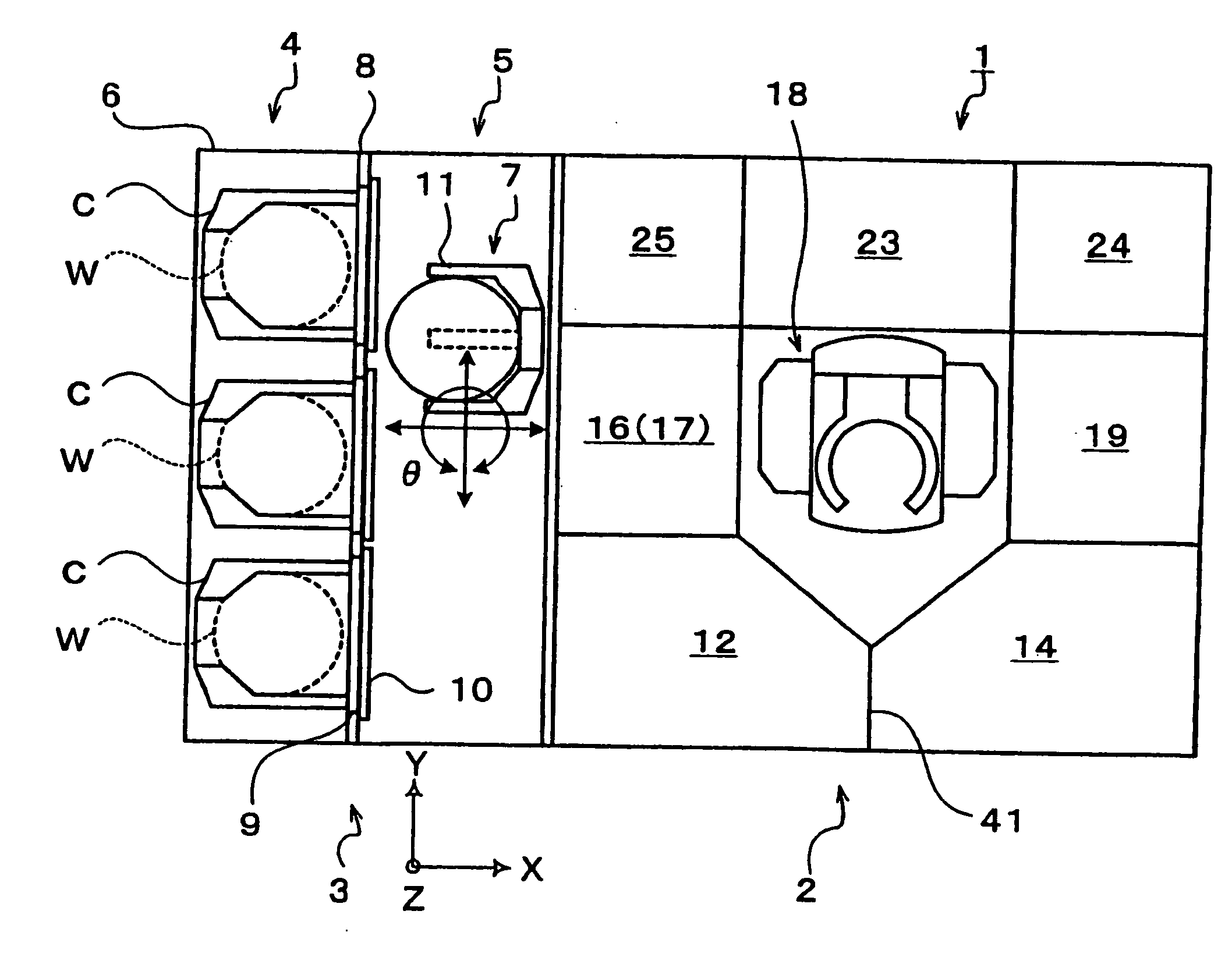
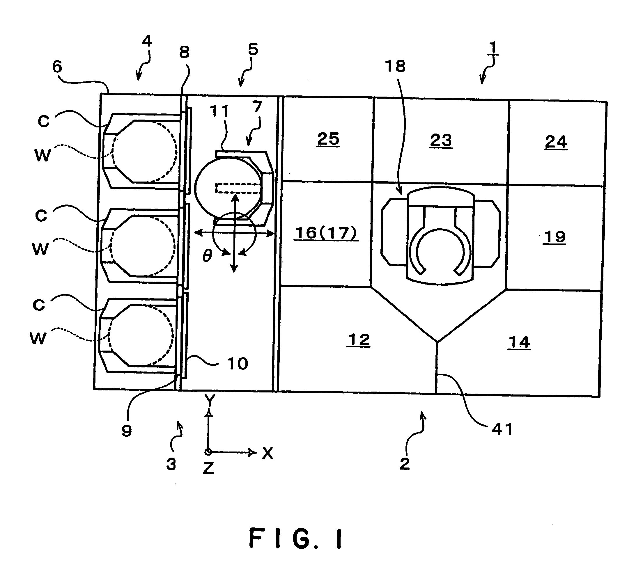
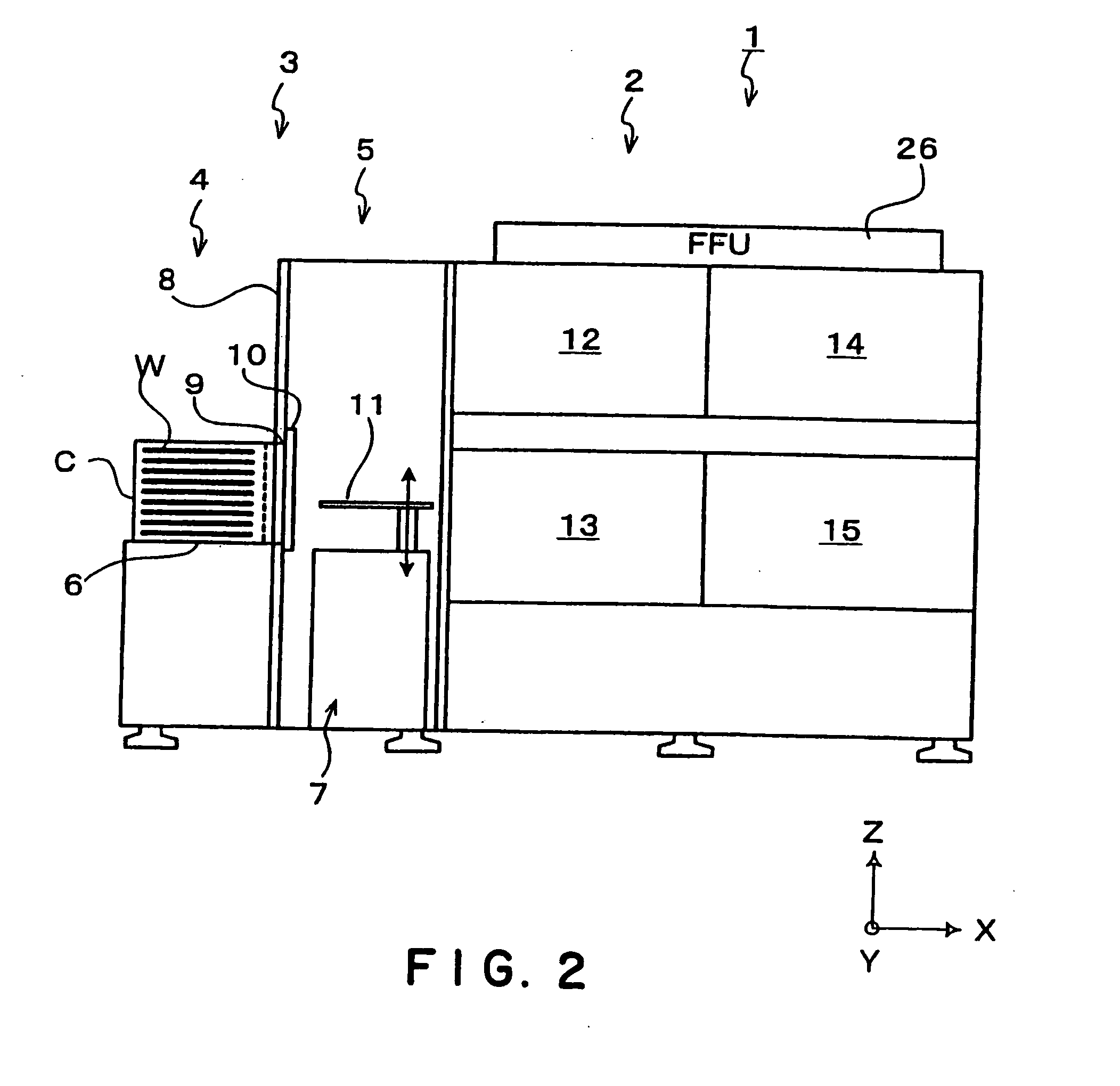
[0056]Based on a substrate processing unit (as the substrate processing apparatus) which is constructed so as to clean the peripheral part of a wafer (as the substrate) and its back face, one preferred embodiment of the present invention will be described below. In the following descriptions, a word “cleaning process” contains a cleaning operation to eliminate a film deposited on a substrate. FIG. 1 is a plan view of the cleaning system 1 having built-in substrate processing units 12, 13 of the embodiment. FIG. 2 is a side view of FIG. 1. The cleaning system 1 includes a cleaning part 2 for carrying out cleaning process for wafers W and sequent heat treatment after cleaning and a loading / unloading part 3 for loading and unloading the wafers W to and from the cleaning part 2.

[0057]The loading / unloading part 3 is formed by an in / out port 4 provided with a mounting table 6 for mounting a container (carrier C) thereon and a wafer-transfer part 5 equipped with a wafer transfer unit 7 for...


PUM


Abstract

A substrate processing apparatus is provided. The apparatus includes a plurality of fluid suppliers 61, 61, 63 for supplying different processing fluids. In processing a wafer W, the substrate processing apparatus moves the fluid suppliers 61, 62, 63 along the peripheral part of the wafer W relatively. The fluid suppliers 61, 62, 63 are arranged in a direction extending from the circumference of the wafer W to its inside. With the arrangement, the apparatus is capable of stable processing of the wafer W in spite of rotating the wafer W at a low speed. Further, it is possible to improve a throughput of the apparatus in resist processing.

Description

BACKGROUND OF THE INVENTION[0001]1. Technical Field of the Invention[0002]This invention relates to substrate processing apparatus for processing substrates, for example, semiconductor wafers, glass substrates for LCD, etc.[0003]2. Description of the Related Art[0004]In the manufacturing process for semiconductor devices, there exists a problem that when a semiconductor wafer (referred as “wafer”, hereinafter) has a metallic film laminated thereon, the metallic film is easy to separate from the peripheral part of the wafer. If such a separation originates in the peripheral part of the wafer, the separation may spread gradually to extend over an area where a semiconductor device is to be built. In order to prevent the occurrence of the above phenomenon, there has been attempted a step of removing a metallic film (part) formed on the peripheral part of the wafer in advance. Note, this removal step will be referred “peripheral-part removing process”, hereinafter. FIG. 21 is an explanat...

Claims


Application Information

Patent Timeline
Patent Type & Authority Applications(United States)
IPC IPC(8): B08B3/00B05C9/12B05C11/08B05C11/10B05D1/40B05D3/00B05D3/10B08B3/02H01L21/00H01L21/304H01L21/306
CPCH01L21/6708B08B3/02H01L21/00
Inventor ORII, TAKEHIKONISHIDA, TATSUYAKURODA, OSAMU
Owner TOKYO ELECTRON LTD
Why Eureka
Try Eureka