High-Frequency Acoustic Wave Device

a high-frequency acoustic wave and propagation device technology, applied in piezoelectric/electrostrictive transducers, generators/motors, transducer types, etc., can solve problems such as limited operation frequency of surface acoustic wave devices, and difficult to further miniaturize conductive combs

Active Publication Date: 2008-09-04
CENT NAT DE LA RECHERCHE SCI +1
View PDF11 Cites 25 Cited by
  • Summary
  • Abstract
  • Description
  • Claims
  • Application Information

AI Technical Summary

Benefits of technology

[0009]An object of the present invention is to provide an acoustic wave device allowing for the

Problems solved by technology

However, such devices raise practical implementation problems when their operating frequency increases.
It is in practice difficult to further miniaturize conductive combs, on the one hand for lithography reasons, and on the other hand for electric loss reason

Method used


Image

  • High-Frequency Acoustic Wave Device
  • High-Frequency Acoustic Wave Device
  • High-Frequency Acoustic Wave Device

Examples


Embodiment Construction

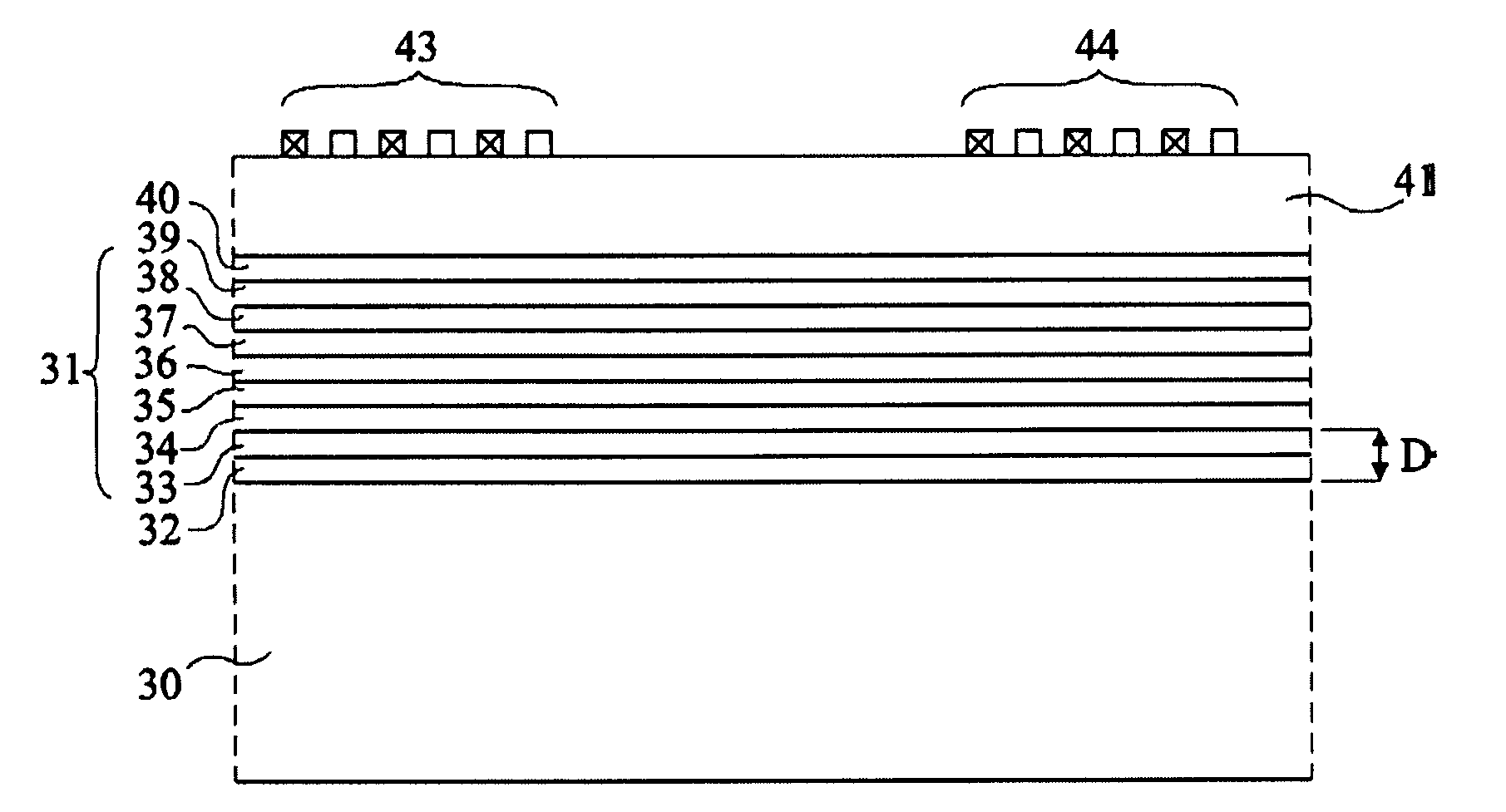
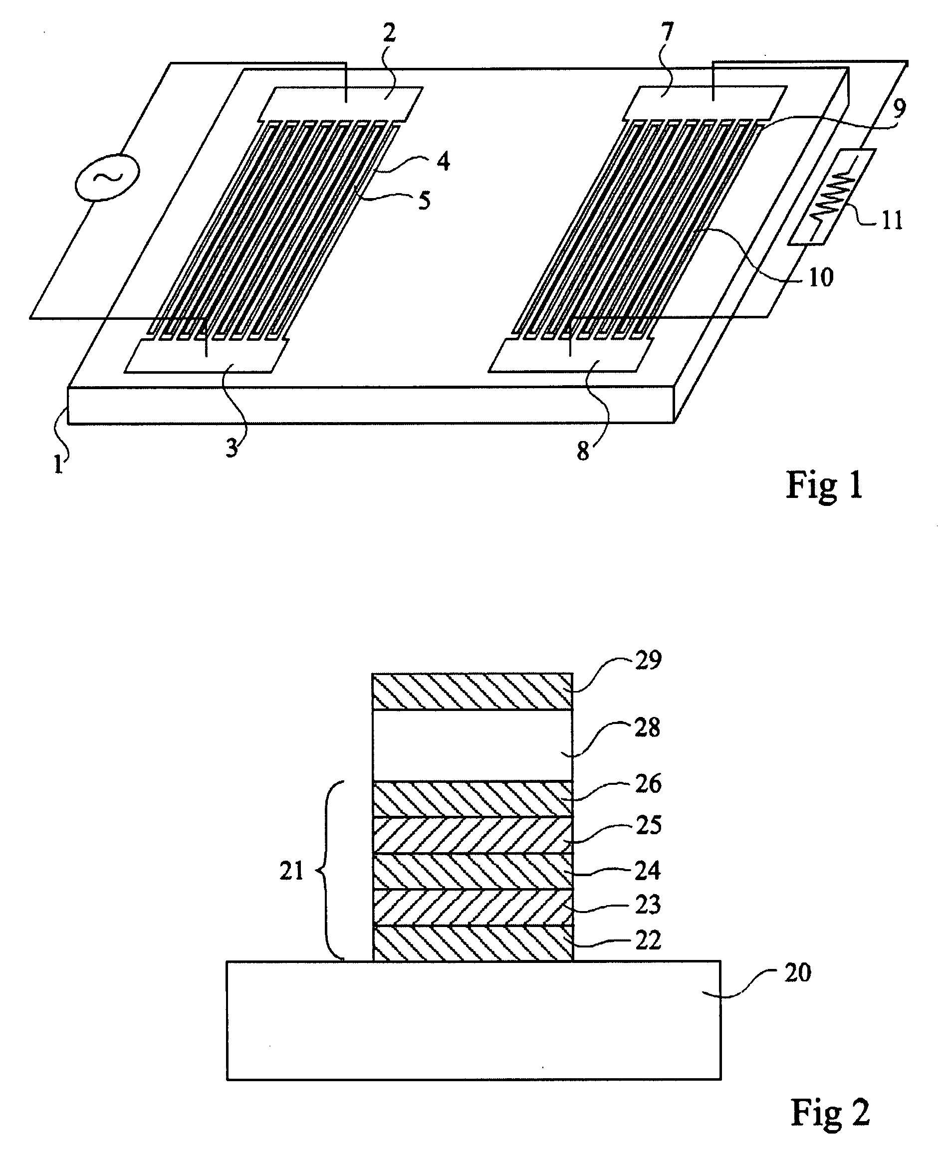
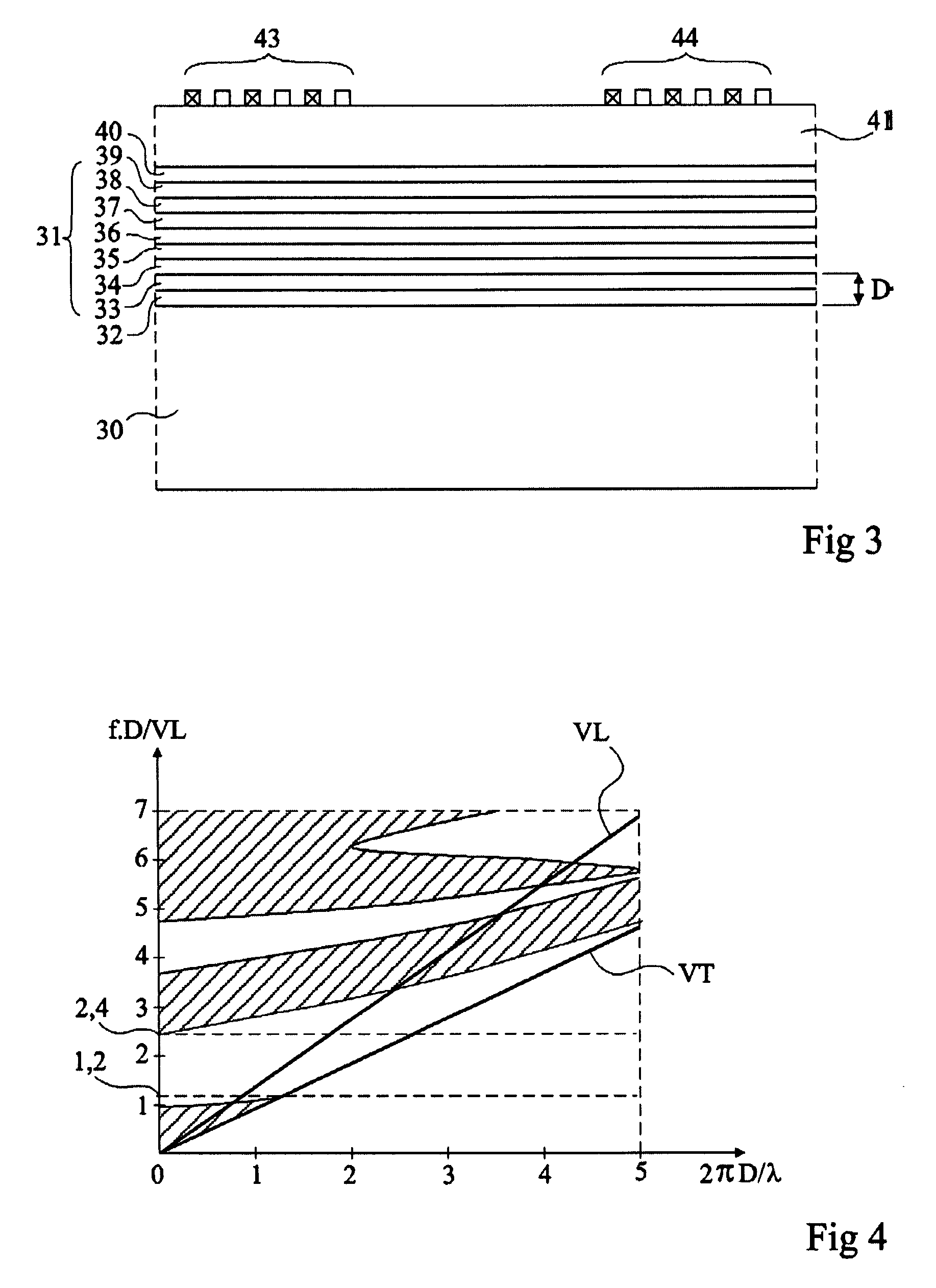
[0024]FIG. 3 shows an embodiment of an acoustic wave device according to the present invention. This device comprises a substrate 30 topped with an acoustic mirror 31 formed of an assembly of layers 32 to 40, the layers with an even reference numeral being of a first material and the layers with an odd reference numeral being of a second material, the two materials having clearly different acoustic impedances. A silicon substrate 30 and a mirror formed of an alternation of tungsten and aluminum layers may for example be used. Above the acoustic mirror is arranged a piezoelectric layer 41, for example, made of aluminum nitride, AlN, or of zinc oxide, ZnO. On piezoelectric layer 41 are arranged surface excitation means, for example, two excitation combs with interdigital teeth 43 and two reception combs with interdigital teeth 44 to form an acoustic wave delay line similar to that described in relation with FIG. 1.

[0025]The inventors have shown that, with such a structure, provided th...


PUM

PropertyMeasurementUnit
Thicknessaaaaaaaaaa
Band gapaaaaaaaaaa
Electrical conductoraaaaaaaaaa

Abstract

An acoustic wave device comprising a piezoelectric layer on an omnidirectional acoustic mirror and excitation and/or reception means on a surface of said piezoelectric layer, capable of exciting waves in a band gap of the acoustic mirror.

Description

FIELD OF THE INVENTION[0001]The present invention relates to the field of acoustic wave propagation devices mainly used in electronics to form resonant systems, filters, delay lines, etc.[0002]Such devices are especially used in the field of high frequencies, currently up to a few gigahertzes, and especially find applications in the field of transmissions, of television, of cell phones, of sensors, and of product labeling tags.DISCUSSION OF PRIOR ART[0003]Two types of acoustic wave devices can be distinguished: surface acoustic wave devices (SAW) and bulk acoustic wave devices (BAW).[0004]FIG. 1 shows an example of a conventional surface acoustic wave device forming a delay line. This device is formed on a piezoelectric substrate 1, possibly one or several thin piezoelectric layers formed on a thicker substrate. The acoustic waves are transmitted in the substrate from two interdigital combs 2 and 3 comprising respective conductive fingers 4 and 5. If a time-variable or A.C. signal i...

Claims


Application Information

Patent Timeline
IPC IPC(8): H03H9/25H01L41/22H01L41/083
CPCH03H3/04H03H9/02228Y10T29/42H03H9/175H03H9/02574
Inventor KHELIF, ABDELKRIMCHOUJAA, ABDELKRIMLAUDE, VINCENT
Owner CENT NAT DE LA RECHERCHE SCI
Why Eureka
Try Eureka