Laser beam processing machine

a laser beam and processing machine technology, applied in metal working equipment, manufacturing tools, welding/soldering/cutting articles, etc., can solve the problems of electrode melt, electrode hole making, and insufficient productivity of via hole drilling, etc., to achieve the effect of improving productivity

Active Publication Date: 2008-09-11
DISCO CORP
View PDF10 Cites 12 Cited by
  • Summary
  • Abstract
  • Description
  • Claims
  • Application Information

AI Technical Summary

Benefits of technology

[0015]In the laser beam processing machine of the present invention, one pulse of a pulse laser beam is applied each time to a plurality of predetermined processing position coordinates to be processed sequentially and a pulse laser beam is applied to a plurality of predetermined processing position coordinates to be processed a predetermined number of times sequentially repeatedly. Therefore, even when the repetition frequency of a pulse laser beam oscillated from the laser beam oscillation means is set to a large value, the time interval between pulses of a pulse laser beam applied to the same electrode position can be made a desired value or more, thereby making it possible to improve productivity.

Problems solved by technology

However, the diameters of the via holes formed in the semiconductor wafer are as small as 30 to 100 μm and hence, drilling of the via holes is not always satisfactory in terms of productivity.
When a via hole reaching the electrode is formed by applying a predetermined number of pulses of the pulse laser beam to the substrate of the wafer, heat generated by the application of the pulse laser beam accumulates in the electrode and reaches the melting point of the electrode, whereby there is caused a problem that the electrode melts and a hole is made in the electrode.
When the time interval between pulses of the pulse laser beam is set to 150 μs or more, however, if the repetition frequency is set to 6,600 Hz or less or 6,600 Hz or more, the number of pulses to be applied to the workpiece must be thinned, which is not always satisfactory in terms of productivity.

Method used


Image

  • Laser beam processing machine
  • Laser beam processing machine
  • Laser beam processing machine

Examples


Embodiment Construction

[0025]A preferred embodiment of a laser beam processing machine constituted according to the present invention will be described in more detail hereinunder with reference to the accompanying drawings.

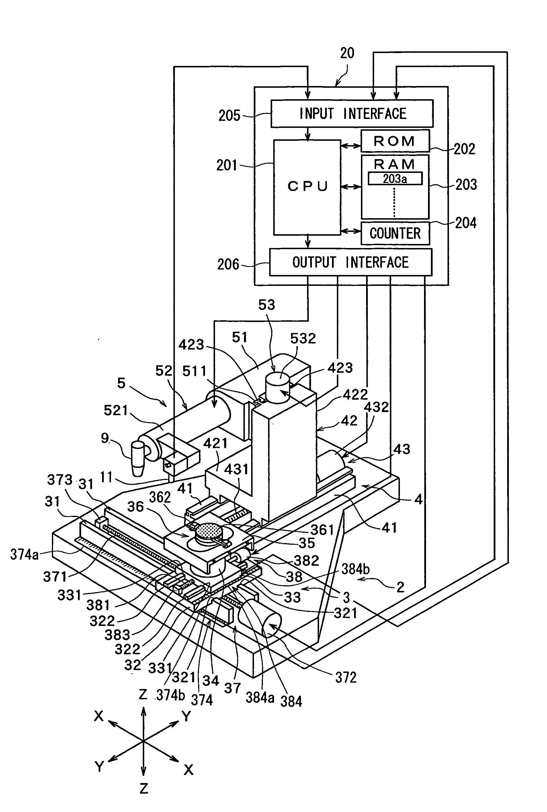
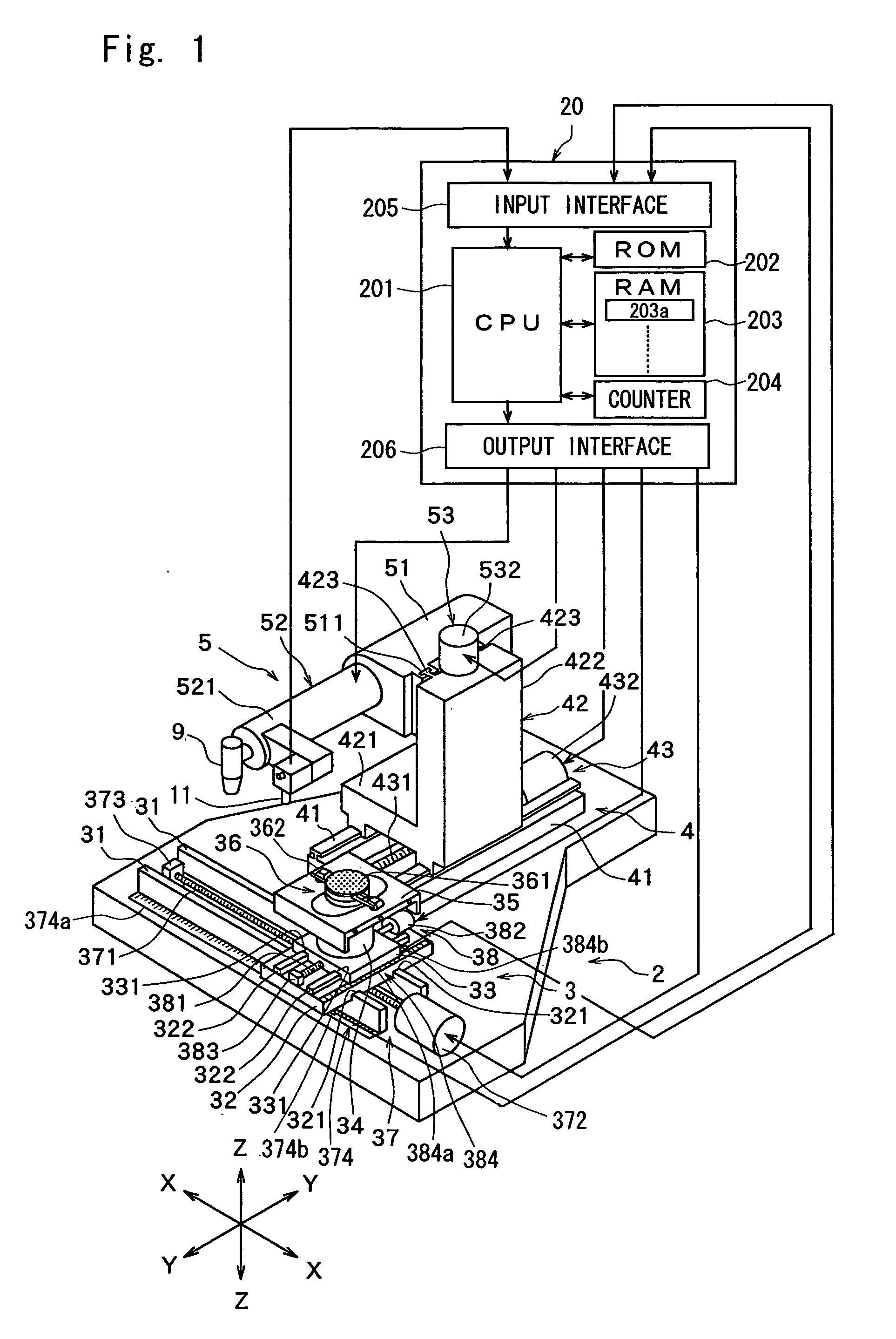
[0026]FIG. 1 is a perspective view of a laser beam processing machine constituted according to the present invention. The laser beam processing machine shown in FIG. 1 comprises a stationary base 2, a chuck table mechanism 3 for holding a workpiece, which is mounted on the stationary base 2 in such a manner that it can move in a processing-feed direction (X direction) indicated by an arrow X, a laser beam application unit support mechanism 4 mounted on the stationary base 2 in such a manner that it can move in an indexing-feed direction (Y direction) indicated by an arrow Y perpendicular to the processing-feed direction (X direction) indicated by the arrow X, and a laser beam application unit 5 mounted on the laser beam application unit support mechanism 4 in such a manner that it can m...


PUM

PropertyMeasurementUnit
timeaaaaaaaaaa
diametersaaaaaaaaaa
thickaaaaaaaaaa

Abstract

A laser beam processing machine comprising a laser beam application means for applying a pulse laser beam to a workpiece held on a chuck table and a controller, wherein the laser beam application means comprises a laser beam oscillation means for oscillating a pulse laser beam, an optical axis changing means for deflecting the optical axis of a pulse laser beam oscillated from the laser beam oscillation means in the processing-feed direction, and a condenser for converging a pulse laser beam whose optical axis has been deflected by the optical axis changing means; and the controller comprises a memory for storing a plurality of processing position coordinates set in the workpiece, controls the optical axis changing means according to the frequency of a pulse laser beam oscillated from the laser beam oscillation means and determines a plurality of predetermined processing position coordinates to be processed to ensure that the time interval between pulses of the pulse laser beam to be applied to the same processing position coordinates becomes a predetermined time or more when one pulse of the pulse laser beam is applied each time to a plurality of predetermined processing position coordinates to be processed sequentially and the pulse laser beam is applied to a plurality of predetermined processing position coordinates to be processed a predetermined number of times sequentially repeatedly.

Description

FIELD OF THE INVENTION [0001]The present invention relates to a laser beam processing machine capable of forming a via hole reaching a bonding pad (electrode) efficiently in a wafer having a plurality of devices on the front surface of a substrate and bonding pads (electrodes) on each of the devices, by applying a pulse laser beam from the rear surface of the substrate.DESCRIPTION OF THE PRIOR ART [0002]In the production process of a semiconductor device, a plurality of areas are sectioned by dividing lines called “streets” arranged in a lattice pattern on the front surface of a substantially disk-like semiconductor wafer, and a device such as IC or LSI is formed in each of the sectioned areas. Individual semiconductor chips are manufactured by cutting this semiconductor wafer along the dividing lines to divide it into the areas in each of which a device is formed.[0003]To reduce the size and increase the number of functions of an apparatus, a modular structure for connecting the el...

Claims


Application Information

Patent Timeline
Patent Type & Authority Applications(United States)
IPC IPC(8): B23K26/02B23K26/00B23K26/04B23K26/08B23K26/382
CPCB23K26/032B23K26/034B23K26/04B23K26/06B23K26/0084B23K26/0869B23K26/4075B23K2201/40B23K26/0853B23K26/40B23K2101/40B23K2103/50B23K26/355
Inventor NOMARU, KEIJIKOBAYASHI, YUTAKAMORIKAZU, HIROSHI
Owner DISCO CORP
Why Eureka
Try Eureka