Active device array substrate and repairing method thereof

Inactive Publication Date: 2008-09-11
CHUNGHWA PICTURE TUBES LTD
View PDF2 Cites 7 Cited by
  • Summary
  • Abstract
  • Description
  • Claims
  • Application Information

AI Technical Summary

Benefits of technology

[0016]One object of the present invention is to provide a simple active device array substrate and an easy repairing method thereof. The pattern layer of the drain electrode has an extended porti

Problems solved by technology

Consequently, the fabrication process is becoming more and more complex and difficult because of the large-scale design.
In the influence of the display quality of the panel, it is hard to give consideration to both the constraint conditions and the process errors at the same time.
During the procedures of fabricating the active device array substrate, the static electricity and the unexpected particle pollution are easily occurring to result in an abnorma

Method used


Image

  • Active device array substrate and repairing method thereof
  • Active device array substrate and repairing method thereof
  • Active device array substrate and repairing method thereof

Examples


first embodiment

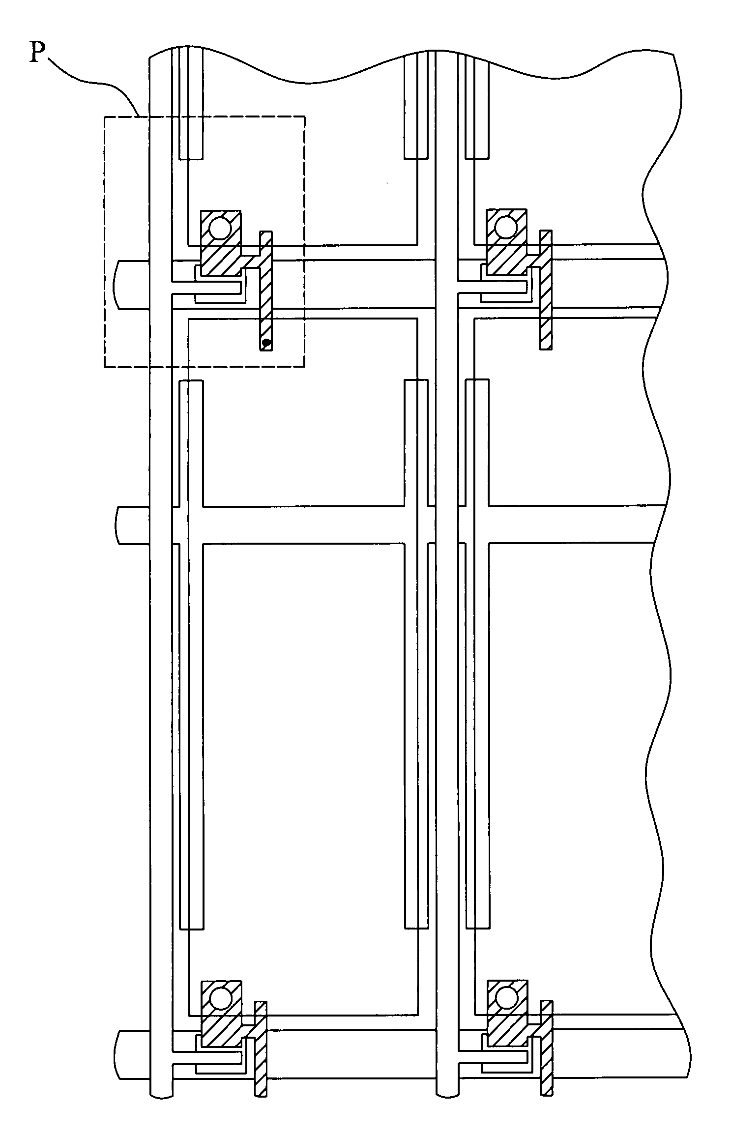
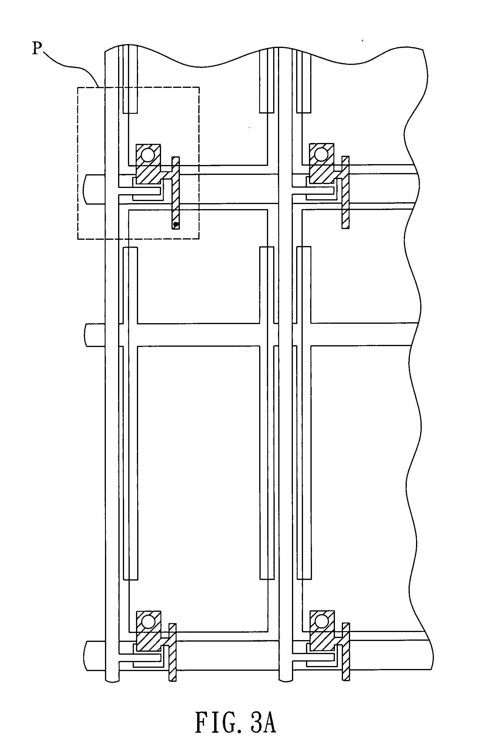
[0032]FIG. 3A is a top-view schematic diagram of partial pixels with the laser repairing structures in an active device array substrate according to the present invention. The active device array substrate comprises a plurality of pixel structures configured in arrays on the substrate.

[0033]FIG. 3B is an amplified schematic diagram of the partial pixels “P” in FIG. 3A. Each of pixel structures includes an active device and a pixel electrode 312. The active device includes at least two metal layers. The first metal layer includes a scan line 304, a storage capacitance line 310 and a pattern layer of a gate electrode (not shown in the figure). The scan line 304 has a portion of gate electrode (not shown in the figure) located under a channel layer 302, the scan signal is transmitted to the gate electrode by the scan line 304. The scan line 304 extends in a row direction. The storage capacitance line 310 is to transmit a common voltage. The second metal layer includes a data line 314, ...

second embodiment

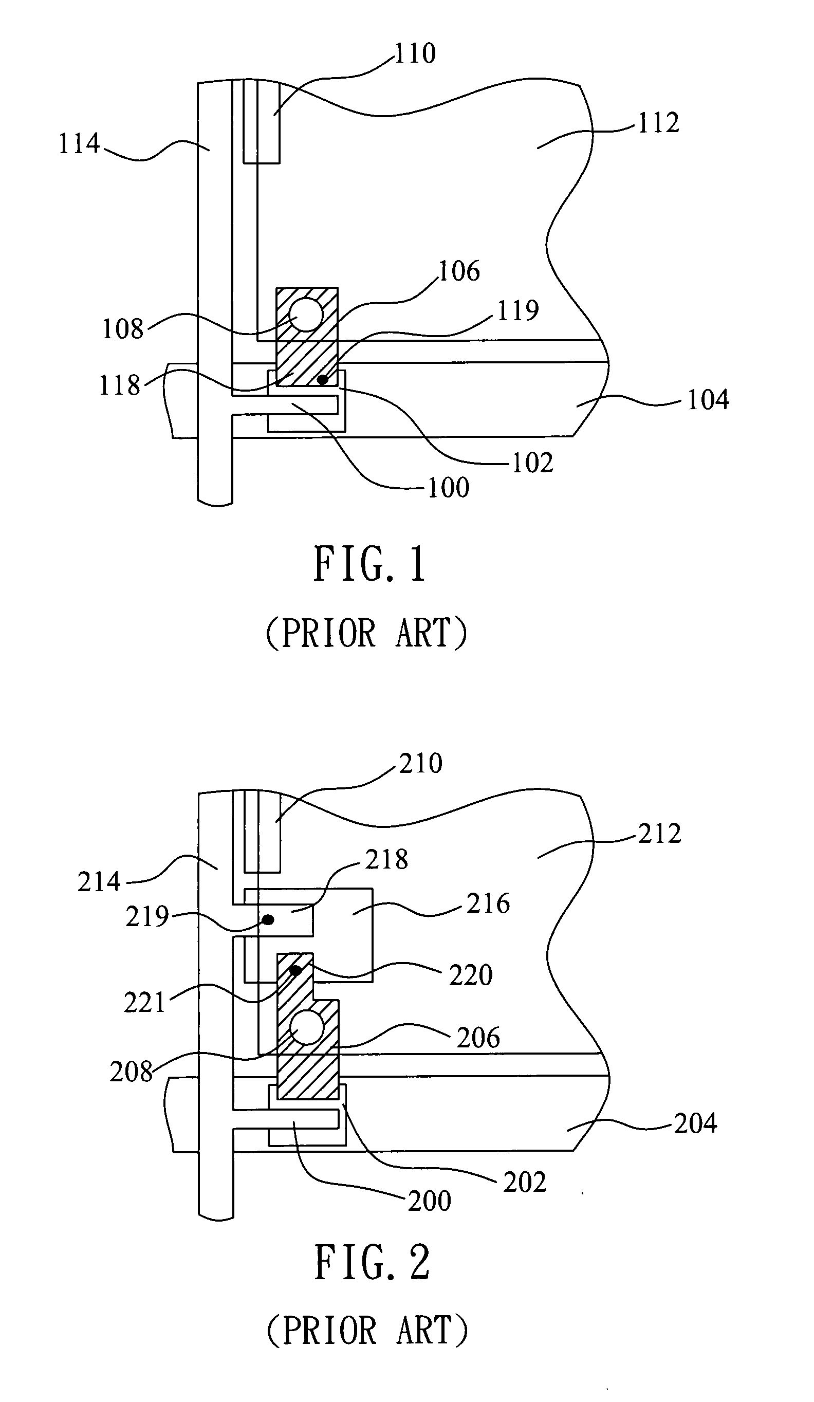
[0043]Nevertheless, the pixel structure and repairing method of the present invention to repairing a white defect by changing it to have the same brightness and color of the adjacent pixel is suitable for many different kinds of pixel structure design for the active device array substrate. the present invention is illustrated in FIG. 4A. The scan line 404 has an extended pattern layer of a gate electrode 405 and a protrusion 407. The gate electrode (not shown in the figure) is included in the extended pattern layer of the gate electrode 405. The pattern layer of the source electrode 301 has a curved concavity and is extended from the data line 314. The second extended portion 408 of the pattern layer of the drain electrode 406 is extended into the curved concavity of the pattern layer of the source electrode 301. The third extended portion 410 of the pattern layer of the drain electrode 406 is extending to a upper side over the protrusion 407 of the scan line 404.

[0044]In this embod...


PUM


Abstract

A simple active device array substrate and an easy repairing method thereof are provided. The pattern layer of the drain electrode has an extended portion extending to the region between an adjacent pixel electrode and the substrate. Once the pixel is found to be a white defect, a laser beam is used to irradiate the overlapped region of the extended portion of the pattern layer of the drain electrode and the adjacent pixel electrode. Then, the current pixel will have the same brightness and color with the adjacent pixel, such that the repairing purpose is achieved.

Description

BACKGROUND OF THE INVENTION[0001]1. Field of the Invention[0002]The present invention relates to an active device array substrate, and more particularly, to a pixel structure of the active device array substrate and the repairing method thereof.[0003]2. Description of the Prior Art[0004]The Thin Film Transistor-Liquid Crystal Display (TFT-LCD) is the most popular Flat Panel Display (FPD) recently because of its many benefits, such as its low power consumption, thin shape, light weight, and low driving voltage, etc.[0005]In recent years, the TFT-LCD has been developed towards to the application field of television, so as the display panel has also been developed towards to the large-scale design. Consequently, the fabrication process is becoming more and more complex and difficult because of the large-scale design. In the influence of the display quality of the panel, it is hard to give consideration to both the constraint conditions and the process errors at the same time.[0006]Gene...

Claims


Application Information

Patent Timeline
IPC IPC(8): H01L29/786H01L21/00
CPCG02F1/136259H01L27/124G02F2001/136268G02F1/136268
Inventor TSOU, YUAN-HSIN
Owner CHUNGHWA PICTURE TUBES LTD
Why Eureka
Try Eureka