[0007]An
advantage of some aspects of the invention is that
power consumption can be reduced, and at the same time, a variation in mobility of a driver transistor can be corrected without reducing an
aperture ratio.
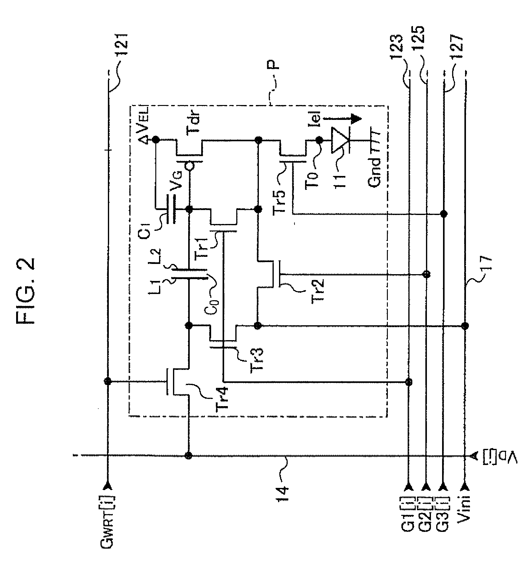
[0009]With this method, in the initialization period, since the first transistor is turned on, the driver transistor is
diode-connected. In such a case, because the second transistor is operated in the saturation region thereof, the gate of the driver transistor is biased at a potential obtained in accordance with the mobility of the driver transistor, thereby obtaining a gate potential of the driver transistor. The gate potential of the driver transistor is maintained across a
gate capacitance thereof. Accordingly, in the writing period, when a data potential corresponding to a gradation is supplied to the other terminal of the capacitive element, the data potential is superimposed on the potential obtained in accordance with the mobility at the gate of the driver transistor, and the superimposed potential is maintained across the
gate capacitance. As a result, the mobility of the driver transistor can be corrected. Furthermore, because no resistor is used, power to be consumed by a resistor can be reduced, and an
aperture ratio can be improved.
[0010]It is preferable that the method for driving a pixel circuit include supplying the fixed potential to the other terminal of the capacitive element and supplying a potential allowing the second transistor to be turned off to the gate of the second transistor in a compensation period provided between the initialization period and the writing period. In the first aspect of the invention, a gate-to-source
voltage of the driver transistor can be approached to the
threshold voltage thereof in the compensation period. More specifically, in a case where the mobility and the
threshold voltage of the second transistor vary, when the initialization period is finished, a gate potential influenced by the characteristic variation of the second transistor is maintained at the gate of the driver transistor. In the compensation period, the gate potential of the driver transistor is changed so as to reach the
threshold voltage thereof. Accordingly, even when the characteristic of the second transistor varies, the negative effect caused by the variation can be reduced. Thus, since the compensation period is provided, the mobility and the threshold
voltage can be corrected. Furthermore, a luminance variation due to the characteristic variation of the second transistor can be suppressed. Any constant potential may be used as the fixed potential. However, when the fixed potential is set to the initialization potential, the number of power supplies can be decreased. Additionally, the compensation period is preferably finished before the gate potential of the driver transistor, i.e., the gate-to-source
voltage, reaches the threshold voltage.
[0012]In the second aspect of the invention, in the initialization period, since the potential of the first
control signal is set to the potential allowing the first transistor to be turned on, the driver transistor is
diode-connected. In this case, since the potential of the second
control signal is set to the predetermined potential allowing the second transistor to be operated in the saturation region thereof, the gate of the driver transistor is biased at a potential obtained in accordance with the mobility thereof, thereby obtaining a gate potential of the driver transistor. The gate potential of the driver transistor is maintained across a
gate capacitance thereof. Accordingly, in the writing period, when the fourth transistor is turned on to supply a data potential corresponding to a gradation to the other terminal of the capacitive element, the data potential is superimposed on the potential obtained in accordance with the mobility at the gate of the driver transistor, and the superimposed potential is maintained across the gate
capacitance. As a result, the mobility of the driver transistor can be corrected. Furthermore, because no resistor is used, power to be consumed by a resistor can be reduced, and an aperture ratio can be improved.
[0014]In the third aspect of the invention, in the compensation period, the potential of the second
control signal is set to the potential allowing the second transistor to be turned off. Accordingly, in the initialization period, the driver transistor is
diode-connected, and the gate of the driver transistor is biased at the initialization potential, thereby obtaining a gate potential of the driver transistor. However, in the compensation period, the gate potential of the driver transistor is changed to a potential obtained by subtracting the threshold voltage of the driver transistor from a potential of the source of the driver transistor. This enables the gate potential of the driver transistor to be changed in accordance with the threshold thereof. As a result, not only the mobility but also the threshold can be corrected. Additionally, since the gate potential of the driver transistor is changed so as to reach the threshold voltage in the compensation period, even when the characteristic of the second transistor varies, the negative effect caused by the variation can be reduced. Furthermore, the compensation period is preferably finished before the gate potential of the driver transistor, i.e., the gate-to-source voltage, reaches the threshold voltage.

