Method of Producing Silicon Blocks and Silicon Wafers

Inactive Publication Date: 2008-09-18
MITSUBISHI ELECTRIC CORP
View PDF8 Cites 35 Cited by
  • Summary
  • Abstract
  • Description
  • Claims
  • Application Information

AI Technical Summary

Benefits of technology

[0010]In a silicon block according to the present invention, by making the content of the alkaline substance be at least 3.5 mass % with respect to the mass of the entire liquid components of said slurry and said slurry contain an organic amine of from 0.5 to 5.0 by a mass ratio with respect to the water in the liquid components of said slurry, and by adjusting the pH of the slurry to be 12 or more, the surface roughness of a cutting surface of the silicon block cut out from the silicon ingot can be made fine.
[0011]Further, a silicon block is cut out from a silicon ingot in such a manner that the surface roughness of a side surface of said silicon block corresponding to an edge face of each of said sliced silicon wafers each having a thickness of 240 μm is 1 μm or less irrespective of the use of such an alkaline slurry, and the surface roughness of a side surface of said silicon block corresponding to an edge face of each of said sliced silicon wafers each having a thickness of 280 μm is less than 3 μm or less. As a result, in the case of producing a solar battery, damage to a substrate is small, similar to the case where a solar battery is formed of silicon wafers sliced to a thickness of 330 μm.

Problems solved by technology

When the bandsaw is used upon cutting out the silicon blocks from the silicon ingot, surfaces of the blocks might be damaged, and if silicon wafers are produced without removing such damaged parts, there arises a problem that cracks might occur in the following processes after the production of the silicon wafers, resulting in a reduction in the yield of the products.

Method used


Image

  • Method of Producing Silicon Blocks and Silicon Wafers
  • Method of Producing Silicon Blocks and Silicon Wafers
  • Method of Producing Silicon Blocks and Silicon Wafers

Examples


Embodiment Construction

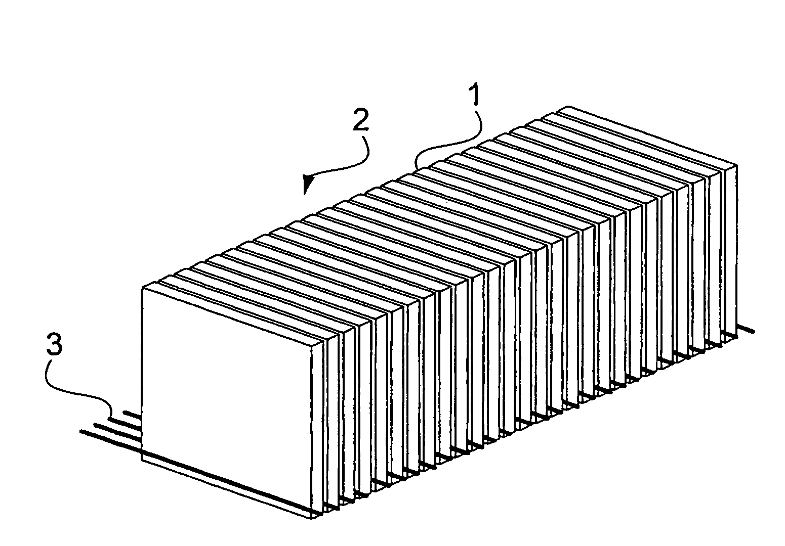
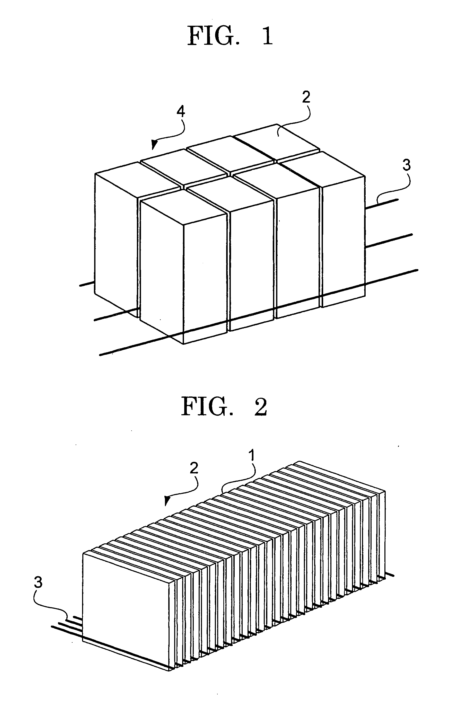
[0015]FIG. 1 is a view that shows the way in which a silicon ingot is cut to silicon blocks in the present invention, and FIG. 2 is a view that shows the way in which a silicon block is sliced to silicon wafers in the present invention.

[0016]The present invention relates to the characteristic of a semiconductor block associated with the production of polysilicon semiconductor wafers used in producing a solar battery. Although silicon is generally widely adopted as such semiconductor, the present invention can also be applied to gallium arsenide alloys, germanium, silicon carbide alloys and the like.

[0017]In the following explanation, description will be made by taking polysilicon as an example.

[0018]As shown in FIG. 1, polysilicon blocks 2 are produced by cutting a polysilicon ingot 4 while supplying a silicon ingot cutting slurry to cutting equipment, and the polysilicon blocks 2 are produced by cutting the polysilicon ingot 4 in such a manner that they have a desired cross-section...


PUM

PropertyMeasurementUnit
Percent by massaaaaaaaaaa
Fractionaaaaaaaaaa
Acidityaaaaaaaaaa

Abstract

In a method of producing silicon blocks by cutting a silicon ingot by the use of a silicon ingot cutting slurry containing abrasive grains and an alkaline substance so as to provide the silicon blocks that can be produced into silicon wafers each having a thin thickness with reduced substrate damage at the time of producing a solar battery, the content of said alkaline substance is at least 3.5 mass % with respect to the mass of the entire liquid components of said slurry, and said slurry contains an organic amine of from 0.5 to 5.0 by a mass ratio with respect to water in the liquid components of said slurry. Said slurry is used at a pH of 12 or more and at a temperature of from 65 to 95 degrees C.

Description

TECHNICAL FIELD[0001]The present invention relates to a method of producing silicon blocks from a polycrystalline ingot for production of a silicon wafer for use with a solar battery, and to a method of producing silicon wafers by using the silicon blocks thus produced by such a producing method.BACKGROUND ART[0002]Polysilicon wafers used to produce solar batteries are manufactured by producing a polysilicon ingot of a quadratic prism, cutting out from the polysilicon ingot a multitude of polysilicon blocks each in the shape of a quadratic prism by the use of a bandsaw, etc., and further by slicing each polysilicon block into quadrangular plates.[0003]When the bandsaw is used upon cutting out the silicon blocks from the silicon ingot, surfaces of the blocks might be damaged, and if silicon wafers are produced without removing such damaged parts, there arises a problem that cracks might occur in the following processes after the production of the silicon wafers, resulting in a reduct...

Claims


Application Information

Patent Timeline
IPC IPC(8): B28D1/00
CPCB28D5/007C09K3/1463B28D5/045Y02P70/10
Inventor MORIKAWA, HIROAKIKARAKIDA, SHOICHIKAWASAKI, TAKAFUMI
Owner MITSUBISHI ELECTRIC CORP
Why Eureka
Try Eureka