Optical Element, Optoelectronic Component Comprising Said Element, and the Production Thereof

a technology of optical elements and optoelectronic components, applied in the field of optical crosslinked polymer formation, can solve the problems of difficult plastics, high cost of materials, and difficult plastics, and achieve the effects of reducing the coefficient of thermal expansion, simple fashion, and reducing the cost of materials

Inactive Publication Date: 2008-09-18
OSRAM OPTO SEMICONDUCTORS GMBH & CO OHG
View PDF23 Cites 34 Cited by
  • Summary
  • Abstract
  • Description
  • Claims
  • Application Information

AI Technical Summary

Benefits of technology

[0006]The advantage of an optical element according to the invention is that it is possible to employ a standard thermoplastic, which by virtue of its thermoplastic properties exhibits a flow transition range above its service temperature and thus, in the softened condition, can be shaped into an optical element in a particularly simple fashion, for example by compression, extrusion, injection molding or injection stamping and other shaping methods. The thermoplastic is then not crosslinked until during or after shaping, the result being a modified thermoplastic that exhibits an elevated heat deflection temperature, a lower coefficient of thermal expansion and improved mechanical properties. Surprisingly, the inventors found that despite crosslinking being performed during or after shaping, optical elements made from these crosslinked thermoplastics exhibit, just as in the prior art, optical properties good enough that the elements can also be employed in optoelectronic systems. The optical elements according to the invention, which comprise the additionally crosslinked thermoplastics, are also surprisingly stable against soldering, so that optoelectronic components that exhibit these elements can be mounted in conventional fashion by soldering to substrates, for example printed circuit boards.

Problems solved by technology

For this reason, high-temperature plastics filled with glass fibers and / or with minerals are used today, which materials are very expensive and can be processed only at high temperatures by special injection molding methods.
These plastics, however, can be shaped only with difficulty.

Method used


Image

  • Optical Element, Optoelectronic Component Comprising Said Element, and the Production Thereof
  • Optical Element, Optoelectronic Component Comprising Said Element, and the Production Thereof
  • Optical Element, Optoelectronic Component Comprising Said Element, and the Production Thereof

Examples


Embodiment Construction

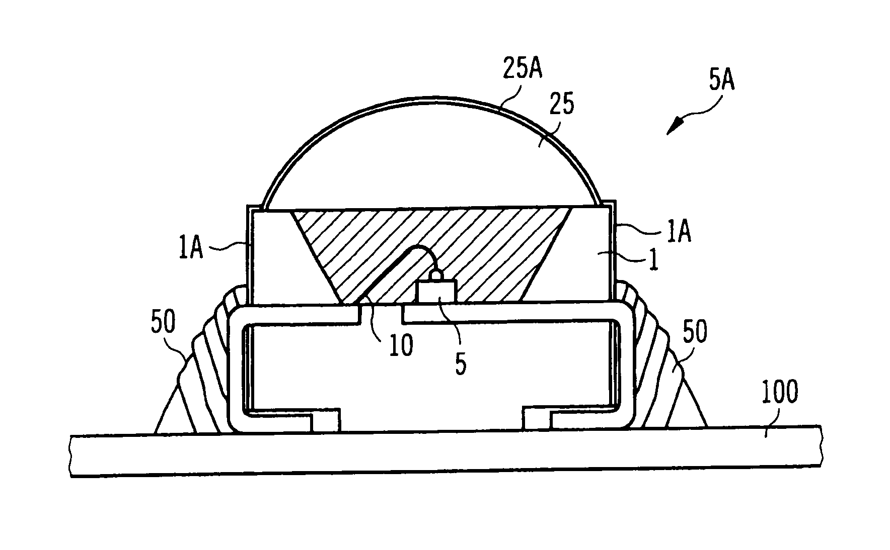
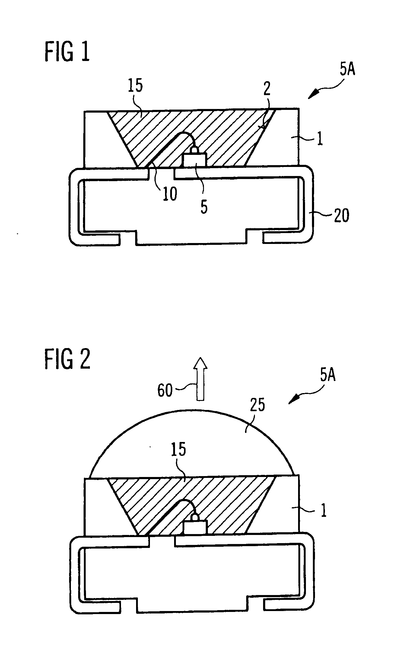
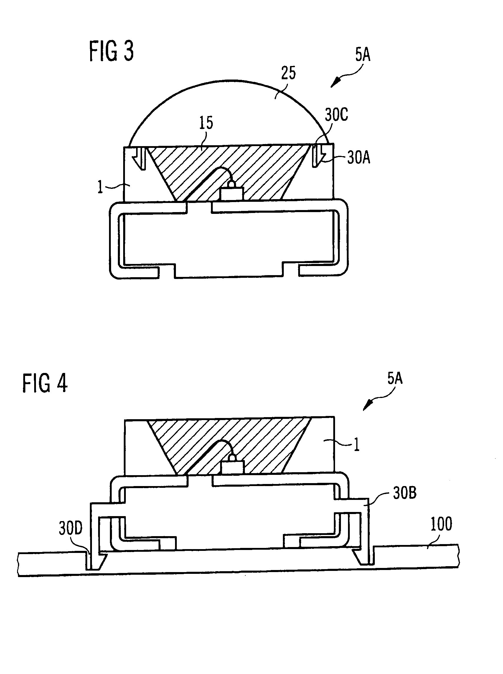
[0015]Optical elements according to the invention can exhibit arbitrary shapes depending on application. Thus for example they can be shaped as packages for the radiation-emitting semiconductor chips, as reflectors or as lenses. The optical elements can thus be given any shape usable for optoelectronic applications. By virtue of the thermoplastic properties, shaping, for example by injection molding, can be carried out in particularly simple fashion, crosslinking not taking place until during or after shaping.

[0016]In a further embodiment of the invention, the expression optical element means an element that interacts with light, that is, in particular, is light-shaping, light-conveying and / or light-transforming. Examples of optical elements are for example lenses that can condense light as well as reflectors that reflect light.

[0017]In an embodiment of the invention it is possible that the thermoplastic is crosslinked by irradiation after shaping. Such irradiation for crosslinking ...


PUM

PropertyMeasurementUnit
thicknessaaaaaaaaaa
transparencyaaaaaaaaaa
thicknessesaaaaaaaaaa

Abstract

The invention relates to an optical element (1, 25) having a defined shape and comprising a thermoplastic material that has been further cross-linked during or following the shaping thereof. Such thermoplastic materials have an increased heat deflection temperature, distortion, but can be easily and economically shaped before the additional cross-linking as a result of the thermoplastic properties thereof.

Description

FIELD OF THE INVENTION[0001]This invention relates to the formation of optical crosslinked polymers which become crosslinked during or after shaping.BACKGROUND AND PRIOR ART[0002]In the case of potting materials for optoelectronic components, such as for example radial LEDs, smart LEDs or chip LEDs, package materials for optoelectronic components such as SMD LEDs or also optical elements such as for example lenses, it is often necessary that the respective materials be stable during soldering. For this reason, high-temperature plastics filled with glass fibers and / or with minerals are used today, which materials are very expensive and can be processed only at high temperatures by special injection molding methods. Thermoset plastics such as epoxy polymers or silicones can be used for encapsulations or optical elements of optoelectronic components. These plastics, however, can be shaped only with difficulty.[0003]It is therefore an object of the invention to identify an optical eleme...

Claims


Application Information

Patent Timeline
Patent Type & Authority Applications(United States)
IPC IPC(8): H01L33/00C08G73/00C08G63/02C08G64/00C08G65/00C08G2/08C08F236/06C08F120/18C08F110/06C08F110/02C08F212/08C08G71/04C08F220/44B29C45/00H01J37/30H01L33/48H01L33/58
CPCH01L33/486H01L33/58H01L2224/48091H01L2224/48247H01L2224/48465Y10T428/265H01L2924/00014H01L2924/00
Inventor KRAUTER, GERTRUDPLOSSL, ANDREAS
Owner OSRAM OPTO SEMICONDUCTORS GMBH & CO OHG
Why Eureka
Try Eureka