Light emitting device and method for manufacturing the same

a technology of light emitting devices and manufacturing methods, which is applied in the manufacture of electrode systems, discharge tube luminescnet screens, lighting and heating apparatus, etc., can solve the problems of failure to provide a light emitting device failure to manufacture the member at a low cost, etc., and achieves low cost manufacturing, low cost, and sufficient electrical insulation

Active Publication Date: 2008-09-18
SHARP KK
View PDF6 Cites 104 Cited by
  • Summary
  • Abstract
  • Description
  • Claims
  • Application Information

AI Technical Summary

Benefits of technology

[0010]The present invention has been made to solve the above-mentioned problems, and its object is to provide a light emitting device that achieves sufficient electrical insulation, and has simple manufacturing processes so that it can be manufactured at a low cost, and a method for manufacturing the same.

Problems solved by technology

Moreover, since light emitting device 101 as shown in FIG. 14 has printed circuit board 104 formed of a glass epoxy substrate, complicated manufacturing processes are required, thereby failing to provide a light emitting device at a low cost.
In Patent Document 2, however, no detailed description is given as to the method for applying the transparent resin used for embedding LED chip 204 and bonding wire W. Moreover, in LED member 201 shown in FIG. 15 of Patent Document 2, since wiring pattern 205 is formed on side faces of wiring board 202 as well as on one portion of the back face, it is difficult to manufacture such a structure, resulting in a failure to manufacture the member at a low cost.

Method used


Image

  • Light emitting device and method for manufacturing the same
  • Light emitting device and method for manufacturing the same
  • Light emitting device and method for manufacturing the same

Examples


Embodiment Construction

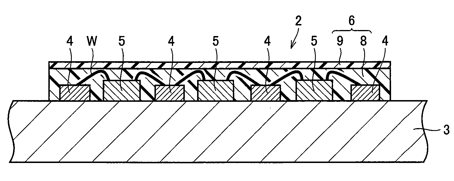
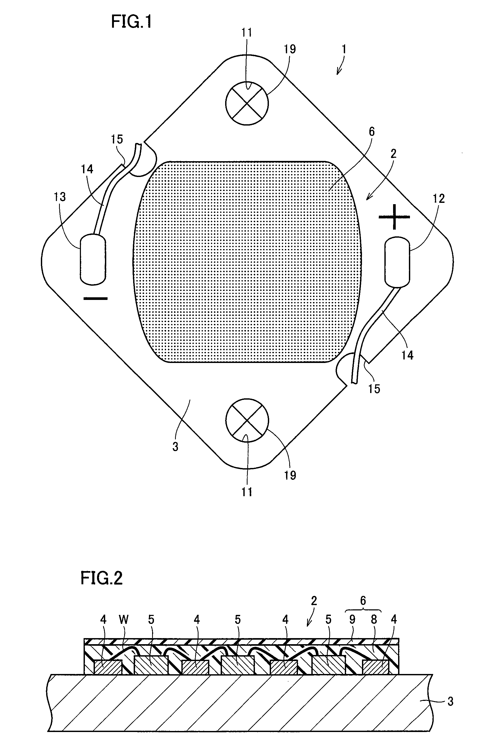
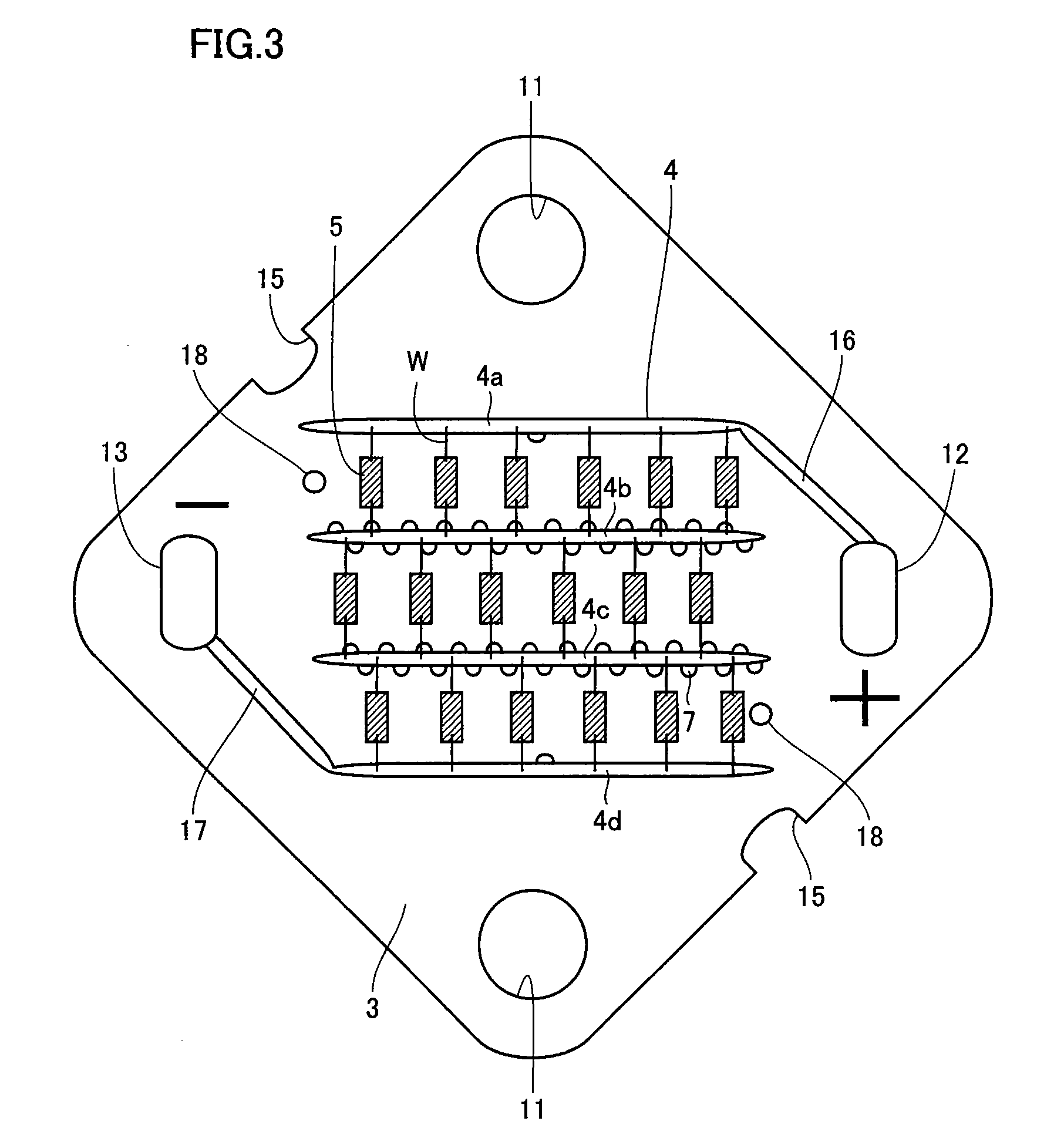
[0043]FIG. 1 is a top view of a light emitting device 1 in accordance with a first preferred example of the present invention, and FIG. 2 is a cross-sectional view schematically showing a light emitting unit 2 in light emitting device 1 of the example shown in FIG. 1. FIG. 3 is a top view schematically showing an insulating substrate 3 in light emitting device 1 of the example shown in FIG. 1. Light emitting device 1 of the present invention has a structure in which a plurality of linear wiring patterns 4 are formed on an insulating substrate 3 in parallel with one another, with a plurality of light emitting elements 5 being mounted between wiring patterns 4 while being electrically connected to wiring patterns 4, and is provided with a light emitting unit 2 sealed by a sealing member 6. In particular, light emitting device 1 of the present invention makes it possible to increase a dielectric voltage between the adjacent light emitting elements as well as between the light emitting ...


PUM


Abstract

By using a light emitting device including an insulating substrate and a light emitting unit formed on the insulating substrate, the light emitting unit including: a plurality of linear wiring patterns disposed on the insulating substrate in parallel with one another, a plurality of light emitting elements that are mounted between the wiring patterns while being electrically connected to the wiring patterns, and a sealing member for sealing the light emitting elements, as well as a method for manufacturing thereof, it becomes possible to provide a light emitting device that achieves sufficient electrical insulation and has simple manufacturing processes so that it can be manufactured at a low cost, and a method for manufacturing the same.

Description

[0001]This nonprovisional application is based on Japanese Patent Application No. 2007-067362 filed with the Japan Patent Office on Mar. 15, 2007, the entire contents of which are hereby incorporated by reference.BACKGROUND OF THE INVENTION[0002]1. Field of the Invention[0003]The present invention relates to a light emitting device and a method for manufacturing the same.[0004]2. Description of the Background Art[0005]In recent years, LEDs have come to be used frequently as light sources for illumination apparatuses. Methods for obtaining white light in the illumination apparatus using LEDs include, for example, a method using three kinds of LEDs, that is, a red LED, a blue LED, and a green LED, and a method utilizing a fluorescent material that converts excited light from a blue LED to emit yellow light. With respect to the light sources for illumination apparatuses, since white light having sufficient luminance is required, illumination apparatuses using a plurality of LED chips h...

Claims


Application Information

Patent Timeline
Patent Type & Authority Applications(United States)
IPC IPC(8): H01J1/02H01J9/02H01L33/32H01L33/48H01L33/50H01L33/54H01L33/56H01L33/62
CPCF21K9/00H01L2924/01047H01L33/62H01L2224/48091H01L2924/09701F21Y2101/02H01L2924/01015F21K9/135H01L2924/3025H01L24/45H01L2924/3011H01L33/36H01L2224/45169H01L2224/45147H01L2224/45144H01L2224/45124H01L2924/01087H01L2924/01068H01L2924/00014H01L2924/00H01L2924/12041F21K9/20F21Y2105/10F21K9/232F21Y2115/10H01L2924/181H01L2224/48465H01L2224/73265H01L2924/00012F21V23/002H01L33/38H01L25/0753H01L33/32H01L33/502H01L33/56H01L33/60H01L33/641
Inventor KONISHI, MASAHIROAGATANI, MAKOTOHATA, TOSHIO
Owner SHARP KK
Why Eureka
Try Eureka