Electric field driving device and electronic apparatus

a driving device and electric field technology, applied in non-linear optics, instruments, optics, etc., can solve the problems of affecting the quality of display, so as to achieve high transmittance ratio and high-quality display

Active Publication Date: 2008-09-18
SEIKO EPSON CORP
View PDF4 Cites 30 Cited by
  • Summary
  • Abstract
  • Description
  • Claims
  • Application Information

AI Technical Summary

Benefits of technology

[0036]According to the above configuration, the electronic apparatus that has a hi...

Problems solved by technology

For this reason, there is a problem that, in proximity to the above end portions of the slits, an electric field is disturbed and, thereby, an alignment state of the liquid crystal is disturbed to thereby produce a domain, or the like, resulting in a decrease in display quality.
In addition, when the number of end portions of the slits is different among a plurality of the sub-pixels corresponding to the...

Method used


Image

  • Electric field driving device and electronic apparatus
  • Electric field driving device and electronic apparatus
  • Electric field driving device and electronic apparatus

Examples


first embodiment

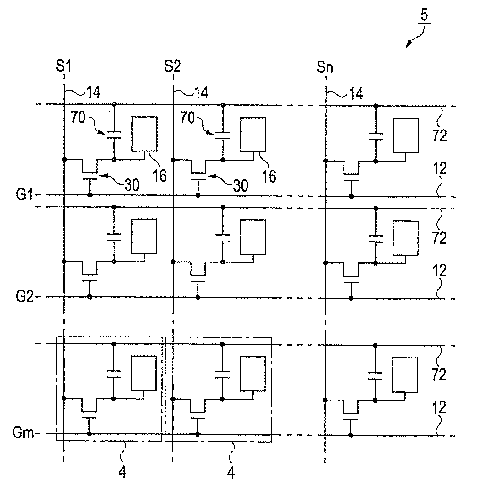
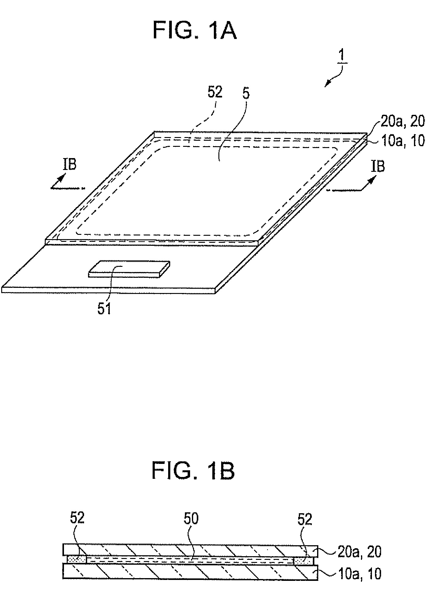
[0056]FIG. 1A is a schematic perspective view of a liquid crystal device, which serves as an electric field driving device, and FIG. 1B is a cross-sectional view that is taken along the line IB-IB in FIG. 1A. The liquid crystal device 1 includes an element substrate 10a and an opposite substrate 20a, which are opposed and adhered to each other through a frame-shaped seal material 52. The element substrate 10a includes a glass substrate 10 as a one substrate, and the opposite substrate 20a includes a glass substrate 20. A liquid crystal 50 is sealed in a space surrounded by the element substrate 10a, the opposite substrate 20a and the seal material 52. The element substrate 10a is larger than the opposite substrate 20a, and is adhered to the opposite substrate 20a in a state where part of the element substrate 10a extends beyond the outer periphery of the opposite substrate 20a. A driver IC 51 that drives the liquid crystal 50 is mounted on the above extended portion. The liquid crys...

second embodiment

[0078]Next, a second embodiment will be described. The liquid crystal device 1 according to the present embodiment differs from that of the first embodiment in that the arrangement of the common electrode 26 and slits 27 and the configuration of the pixels 3 are modified, and the other portions are the same as those of the first embodiment. In the drawings used in the following description, the same reference numerals are assigned to the same components as those of the first embodiment, and the description thereof is omitted.

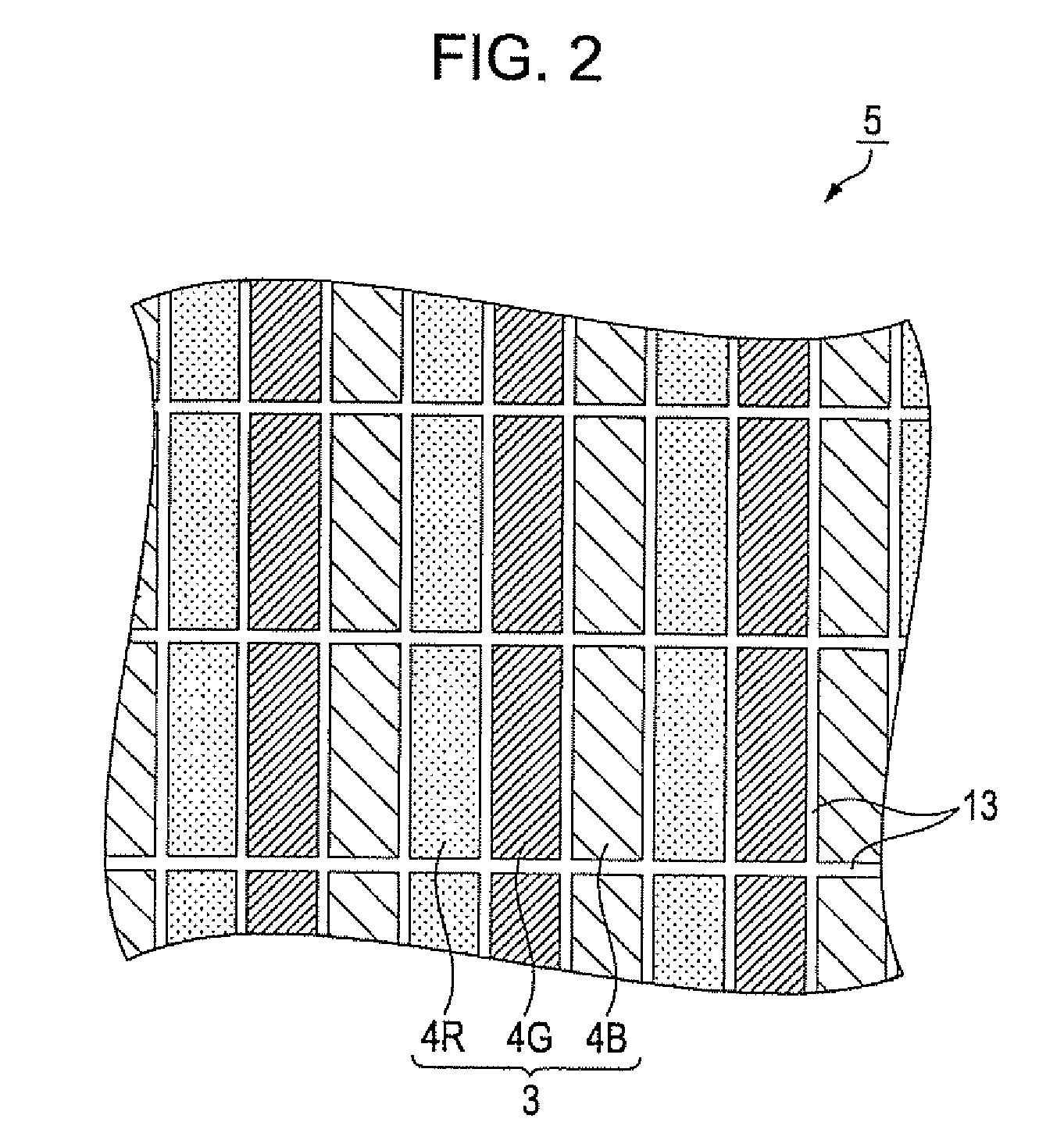
[0079]FIG. 8 is a plan view that specifically shows a portion corresponding to adjacent two pixels 3 within the pixel region 5 of the liquid crystal device 1 according to the present embodiment. Each of the pixels 3 according to the present embodiment is configured so that four-color sub-pixels 4 are arranged along the longitudinal direction of the slits 27. More specifically, each of the pixels 3 is formed of sub-pixels 4R, 4G, 4B, 4C that contribute to display...

third embodiment

[0085]Next, a third embodiment will be described. The present embodiment also differs from the first embodiment in that the arrangement of the common electrode 26 and slits 27 and the configuration of the pixels 3 are modified, and the other portions are the same as those of the first embodiment.

[0086]FIG. 9 is a plan view that specifically shows a portion of the pixel region 5 of the liquid crystal device 1 according to the present embodiment. Each of the pixels 3 in this drawing is configured so that two-color sub-pixels 4 are arranged along the longitudinal direction of the slits 27. More specifically, each of the pixels 3 is formed of sub-pixels 4R, 4G that contribute to displays of red and green.

[0087]In the present embodiment, a set of two pixels 3 that are arranged along the longitudinal direction of the slits 27 is termed as a pixel block 2. The layout of the pixel region 5, including the patterns of the common electrode 26 and slits 27, is configured so that the pixel block...


PUM


Abstract

An electric field driving device, in which a plurality of pixels, each of which is formed of two or more sub-pixels that respectively correspond to different colors from one another, are arranged in a matrix in a pixel region on a substrate, includes pixel electrodes, a common electrode, an insulating layer, and a material. Each of the pixel electrodes is formed in correspondence with the sub-pixel on the substrate. The common electrode is formed above the pixel electrodes on the substrate so that at least part of the common electrode overlaps each of the pixel electrodes in plan view. The insulating layer is formed on the substrate between the pixel electrodes and the common electrode. The material is driven by an electric field that is generated on the basis of a difference in electric potential between each of the pixel electrodes and the common electrode. The common electrode has a plurality of slits that at least partly overlap the pixel electrodes in plan view. At least a portion of the slits are respectively provided continuously over a plurality of the sub-pixels. Each of the sub-pixels corresponding to the same color includes the same numbers of end portions of the plurality of slits.

Description

[0001]This application claims priority from Japanese Patent Application No. 2007-062970 filed in the Japanese Patent Office on Mar. 13, 2007, and Japanese Patent Application No. 2007-298917 filed in the Japanese Patent Office on Nov. 19, 2007, the entire disclosures of which are hereby incorporated by reference in its entirety.BACKGROUND[0002]1. Technical Field[0003]The present invention relates to an electric field driving device and an electronic apparatus.[0004]2. Related Art[0005]A liquid crystal device is one of electric field driving devices and modulates transmitted light by driving a liquid crystal using an electric field. One embodiment of the liquid crystal device has been known as an FFS (Fringe Field Switching) mode liquid crystal device that drives a liquid crystal by a lateral electric field that is parallel to the substrates, which is described in JP-A-2002-296611. The liquid crystal device includes pixel electrodes and a common electrode. The pixel electrodes are pro...

Claims


Application Information

Patent Timeline
IPC IPC(8): G02F1/1343
CPCG02F1/134363G02F2001/134372G02F2001/134318G02F1/134318G02F1/134372G02F1/1362G02F2201/121G02F2201/123
Inventor WAKABAYASHI, JUNICHI
Owner SEIKO EPSON CORP
Why Eureka
Try Eureka