Switching element, method for manufacturing the same, and display device including switching element

a switching element and manufacturing method technology, applied in the direction of relays, semiconductor/solid-state device details, instruments, etc., can solve the problems of large storage capacitor needs, difficult to hold a potential of a pixel electrode, and difficulty in maintaining a completely off-state state, so as to prevent damage and miniaturize the switching element

Inactive Publication Date: 2008-10-02
SEMICON ENERGY LAB CO LTD
View PDF11 Cites 13 Cited by
  • Summary
  • Abstract
  • Description
  • Claims
  • Application Information

AI Technical Summary

Benefits of technology

[0010]In view of the above problems, an object of the present invention is to provide a switching element which has enough resistance even in the case where switching operations are repeated and which can be miniaturized and have low power consumption, a method for manufacturing the switching element, and a display device including the switching element.
[0017]According to the present invention, a switching operation (contact or noncontact operation) is performed by expansion and contraction of an insulating film provided between conductive films, and thus, stress is not concentrated in a portion of a switching element; therefore, the element is prevented from being damaged. Further, since expansion and contraction in up and down directions of the insulating film provided between the conductive films are utilized, it is not necessary to widen a gap 104, and therefore, the switching element can be miniaturized. Further, according to the present invention, since a potential difference between a conductive film which functions as an upper electrode and a conductive film which functions as a lower electrode is constant when the switching element is off, malfunctioning of the switching element can be prevented even in a case where the switching element is driven with low power consumption.

Problems solved by technology

However, active driving has a problem in that because switching on / off of a potential of a pixel electrode is performed electrically using TFTs, an off current (leak current) flows even in an off state and thus it is difficult to maintain a completely off state.
When there is an off current, it is difficult to hold a potential of a pixel electrode.
Further, the higher an off current is, the larger the storage capacitor needs to be.
Thus, problems such as lower driving frequency and a flicker in a screen are caused.
Further, because it is necessary to supply an excess charge to the storage capacitor, power consumption increases.
However, in the case where a switching element is provided so as to have a plate structure in which one side is fixed (Cited Document 1), stress is locally concentrated at the time of switching operation of the switching element (a contact or noncontact operation between an upper electrode and a lower electrode); therefore, damage of the switching element is a problem.
Similarly, in the case where a flexible thin film and a conductive film are bent with the use of a supporting board to perform a contact or noncontact operation (Cited Document 2), stress is also caused in a specific portion of the flexible thin film; therefore, resistance of an element is a problem.
Further, it is necessary to form a somewhat large gap; therefore, it is difficult to miniaturize the switching element.
As for the structure of a piezoelectric switch disclosed in Cited Document 3, even when a switching element is off (an upper electrode and a pixel electrode are not in contact with each other), a potential difference is generated in a piezoelectric element as a signal line which functions as a lower electrode changes, so the switching element cannot be completely turned off, and therefore, malfunction might occur.
In particular, in a case where a gap between the upper electrode and the pixel electrode is small, there is a significant possibility that malfunction might occur.
Meanwhile, in the case where the gap is widened to prevent malfunctions, in order that the switching element be turned on, it is necessary for a potential difference between the upper electrode and the lower electrode to be larger, and thus, power consumption of the switching element increases.
In this case, a potential difference between a wiring connected to the upper electrode and a wiring connected to the lower electrode is also larger; therefore, there is a possibility that a leak current might occur in a portion where the wirings intersect with each other.
Consequently, a display defect might be caused due to reduction in voltage applied to the piezoelectric element as well as increase in power consumption.

Method used


Image

  • Switching element, method for manufacturing the same, and display device including switching element
  • Switching element, method for manufacturing the same, and display device including switching element
  • Switching element, method for manufacturing the same, and display device including switching element

Examples


embodiment mode 1

[0037]In this embodiment mode, a switching element and a display device including the switching element of the present invention will be described with reference to the drawings.

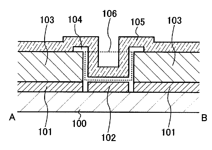
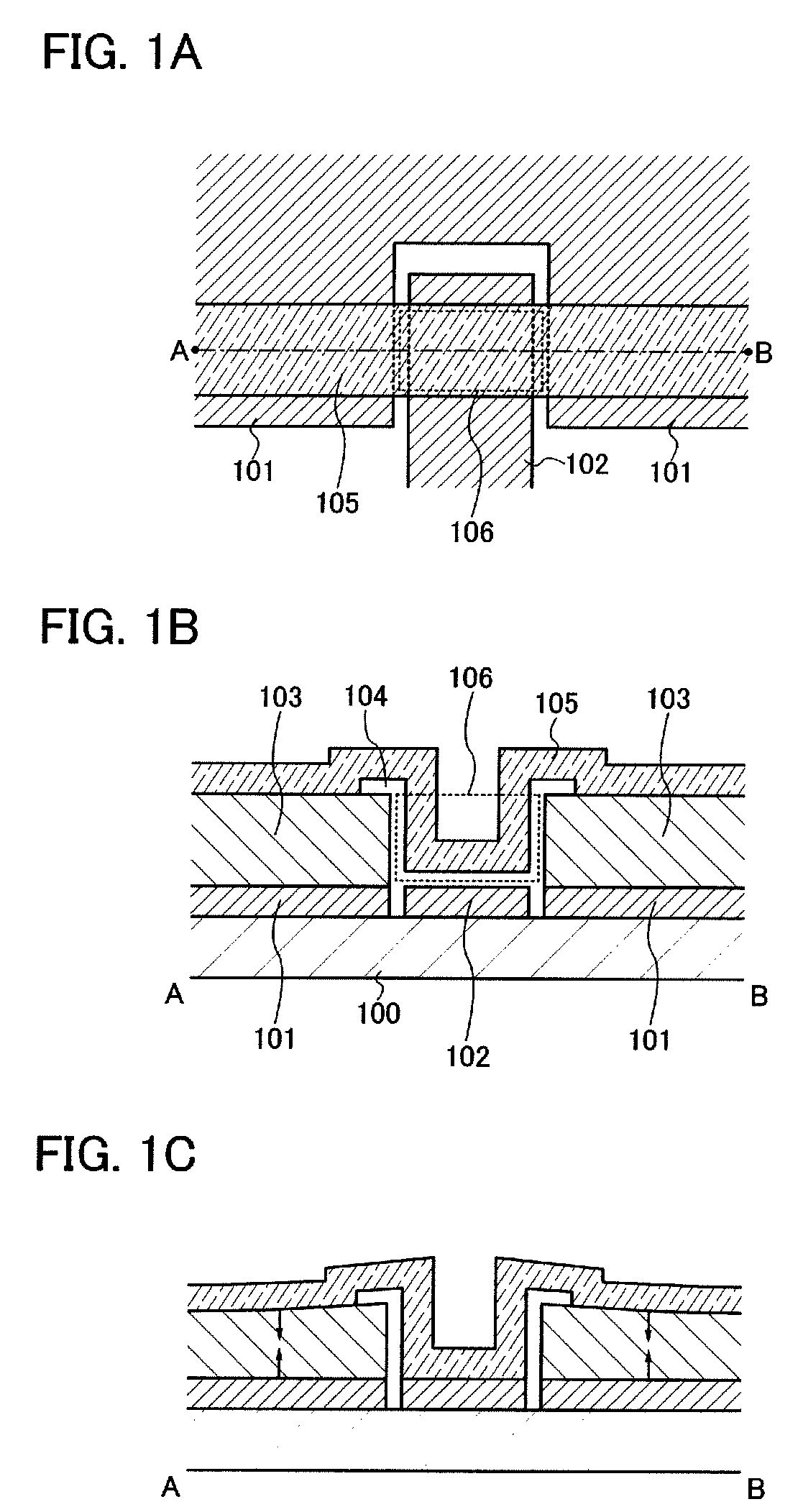
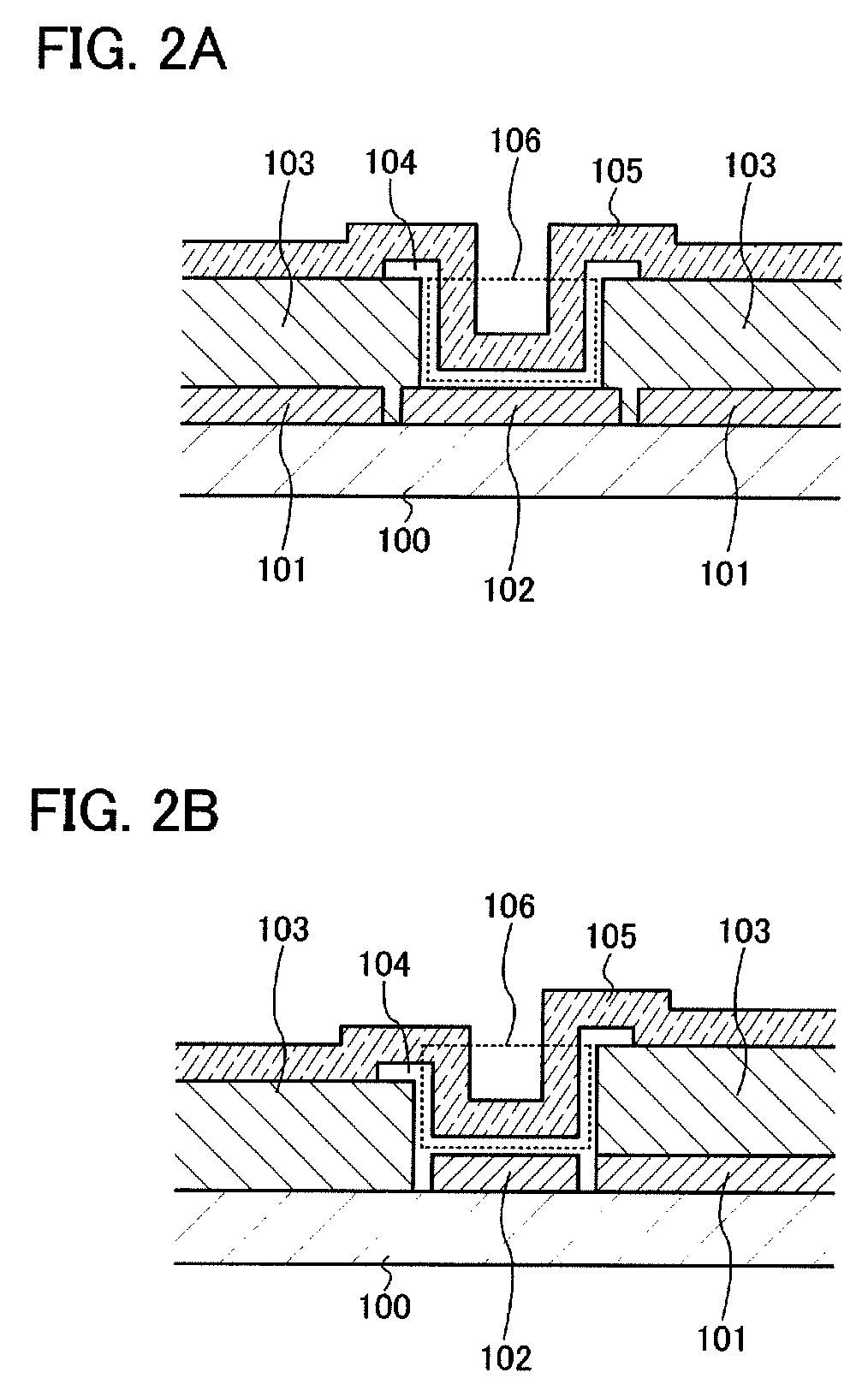
[0038]First, the switching element will be described with reference to FIGS. 1A to 1C. Note that FIG. 1A shows a top plan view of the switching element and FIGS. 1B and 1C show cross-sectional views taken along line A-B in FIG. 1A.

[0039]The switching element includes a first conductive film 101 and a second conductive film 102 which are provided over a substrate 100, an insulating film 103 which functions as a spacer layer, a gap 104, and a third conductive film 105 (see FIGS. 1A and 1B). In the switching element, the first conductive film 101 functions as a first electrode (lower electrode), the third conductive film 105 functions as a third electrode (upper electrode), and the second conductive film 102 functions as a second electrode which is or is not in contact with the third electrode.

[0040]The first c...

embodiment mode 2

[0059]In this embodiment mode, the structure of the display device including the switching element described in the above embodiment mode and a method for manufacturing the display device are described with reference to the drawings.

[0060]First, the structure of the display device described in this embodiment mode is described with reference to FIGS. 4 to 5B. Note that FIG. 4 shows a top plan view of a pixel in the display device, FIG. 5A shows a cross-sectional view taken along line A1-B1 in FIG. 4, and FIG. 5B shows a cross-sectional view taken along A2-B2 in FIG. 4.

[0061]The display device described in this embodiment mode includes a conductive film 205 which can function as a gate line, a conductive film 201 which can function as a common line, a pixel electrode 211, a conductive film 202 which is electrically connected to the pixel electrode 211, a conductive film 221 which can function as a data line, and a counter electrode 222 which is electrically connected to the conductiv...

embodiment mode 3

[0090]In this embodiment mode, a different method for manufacturing a switching element from the above embodiment mode is described with reference to the drawings. In specific, a case of forming a gap without using a sacrificial layer in the method for manufacturing a switching element is described.

[0091]In this embodiment mode, a gap is formed by applying volume contraction due to cohesion. Hereinafter, description is made with reference to FIGS. 13A to 14B.

[0092]First, the first conductive film 101 and the second conductive film 102 are selectively formed over the substrate 100 and then the insulating film 103 which functions as a spacer layer is formed so as to cover the first conductive film 101 and the second conductive film 102 (see FIG. 13A).

[0093]Each of the first conductive film 101 and the second conductive film 102 is formed to have a single-layer structure or a stacked-layer structure using an element selected from aluminum (Al), tungsten (W), titanium (Ti), tantalum (Ta...


PUM

PropertyMeasurementUnit
thicknessaaaaaaaaaa
thicknessaaaaaaaaaa
driving voltageaaaaaaaaaa

Abstract

A method for manufacturing a switching element which has enough resistance to repeat switching operations and which can be miniaturized and have low power consumption, and a display device including the switching element are provided. The switching element includes a first electrode to which a constant potential is applied, a second electrode adjacent to the first electrode, and a third electrode over the first electrode with a spacer layer formed of a piezoelectric material interposed therebetween and provided across the second electrode such that there is a gap between the second electrode and the third electrode. A potential which is different from or approximately the same as a potential of the first electrode is applied to the third electrode to expand and contract the spacer layer, so that a contact state or a noncontact state between the second electrode and the third electrode can be selected.

Description

BACKGROUND OF THE INVENTION[0001]1. Field of the Invention[0002]The present invention relates to a switching element, a method for manufacturing a switching element, and a display device including a switching element. In particular, the present invention relates to a display device including a mechanical switch.[0003]2. Description of the Related Art[0004]In recent years, as a display device using a liquid crystal panel or the like, an active-driving display device using thin film transistors (TFTs) is employed in many cases for higher definition. In the case of an active-driving display device, the potential of each pixel electrode can be independently controlled and thus there is no crosstalk such as a leak of an electrical field to an adjacent pixel, as there is in the case of a passive-driving display device; therefore, a panel with less unevenness in display and a higher contrast ratio can be manufactured.[0005]However, active driving has a problem in that because switching on / ...

Claims


Application Information

Patent Timeline
Patent Type & Authority Applications(United States)
IPC IPC(8): H01H57/00H01H11/00H01H47/22
CPCG02F1/1368Y10T29/49105H01L27/20H01L41/0986H01L2924/0002H01H2057/006H01L41/29H01L41/27H05K3/184H01L23/481H05K3/107H05K3/181H05K3/1258H01L2924/00Y10T29/42Y10T29/49005Y10T29/49126Y10T29/49128Y10T29/49155H10N39/00H10N30/206G02F1/133G02F1/1335H10N30/05H10N30/06
Inventor HONDA, TATSUYA
Owner SEMICON ENERGY LAB CO LTD
Why Eureka
Try Eureka