
Local clock buffer (LCB) with asymmetric inductive peaking

a local clock buffer and inductive peaking technology, applied in logic circuits, pulse techniques, electrical apparatus, etc., can solve the problems of reducing lcb, chip power consumption has increased, chip and system level cooling and packaging costs have increased, etc., to and reduce synchronous ic chip power consumption.

Inactive Publication Date: 2008-10-02
IBM CORP
View PDF2 Cites 2 Cited by
  • Summary
  • Abstract
  • Description
  • Claims
  • Application Information

AI Technical Summary

Benefits of technology

[0011]It is another purpose of the invention to reduce synchronous IC chip power without degrading chip performance;
[0012]It is yet another purpose of the invention to reduce synchronous IC chip power consumed in CMOS clock buffers without degrading chip performance.
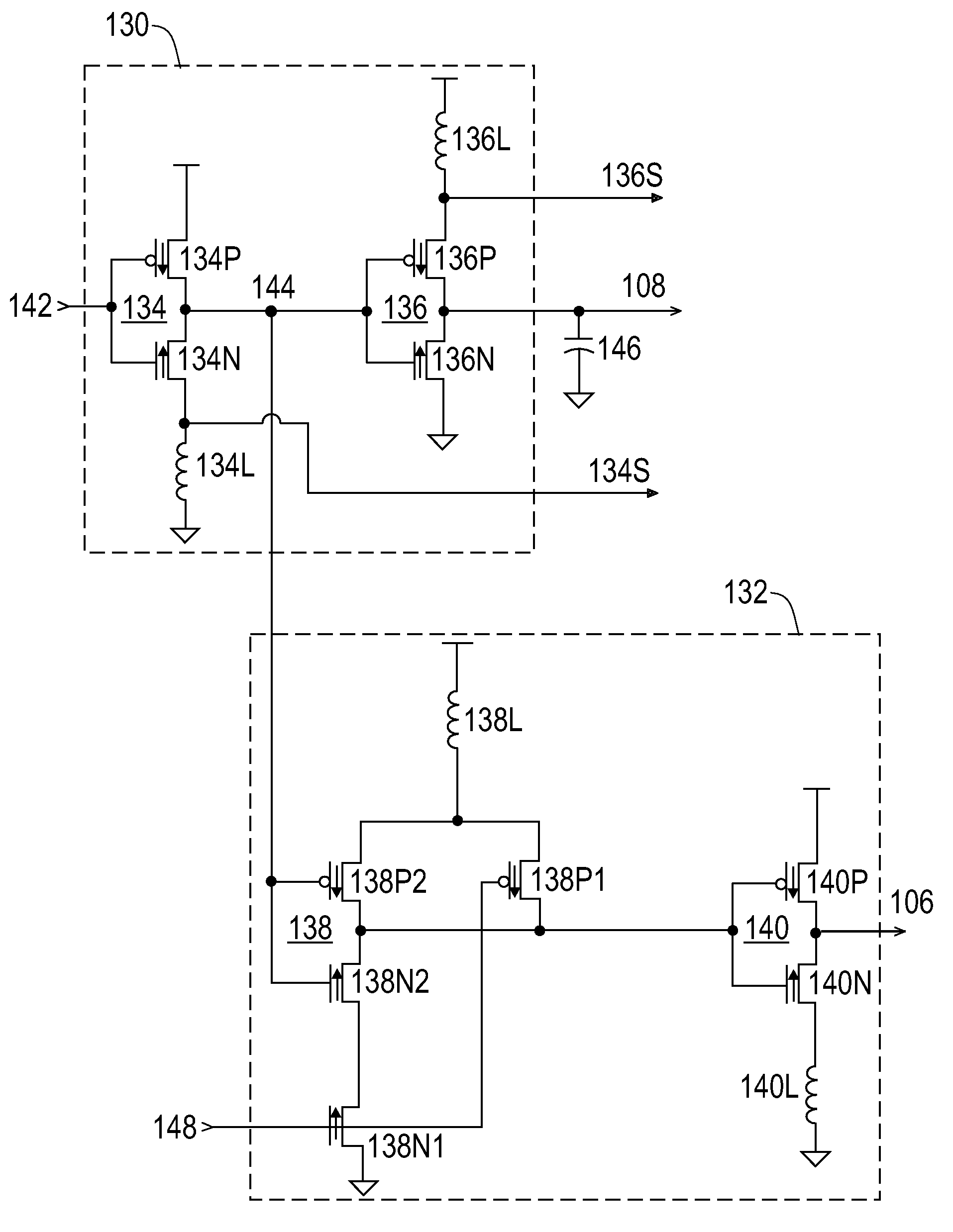
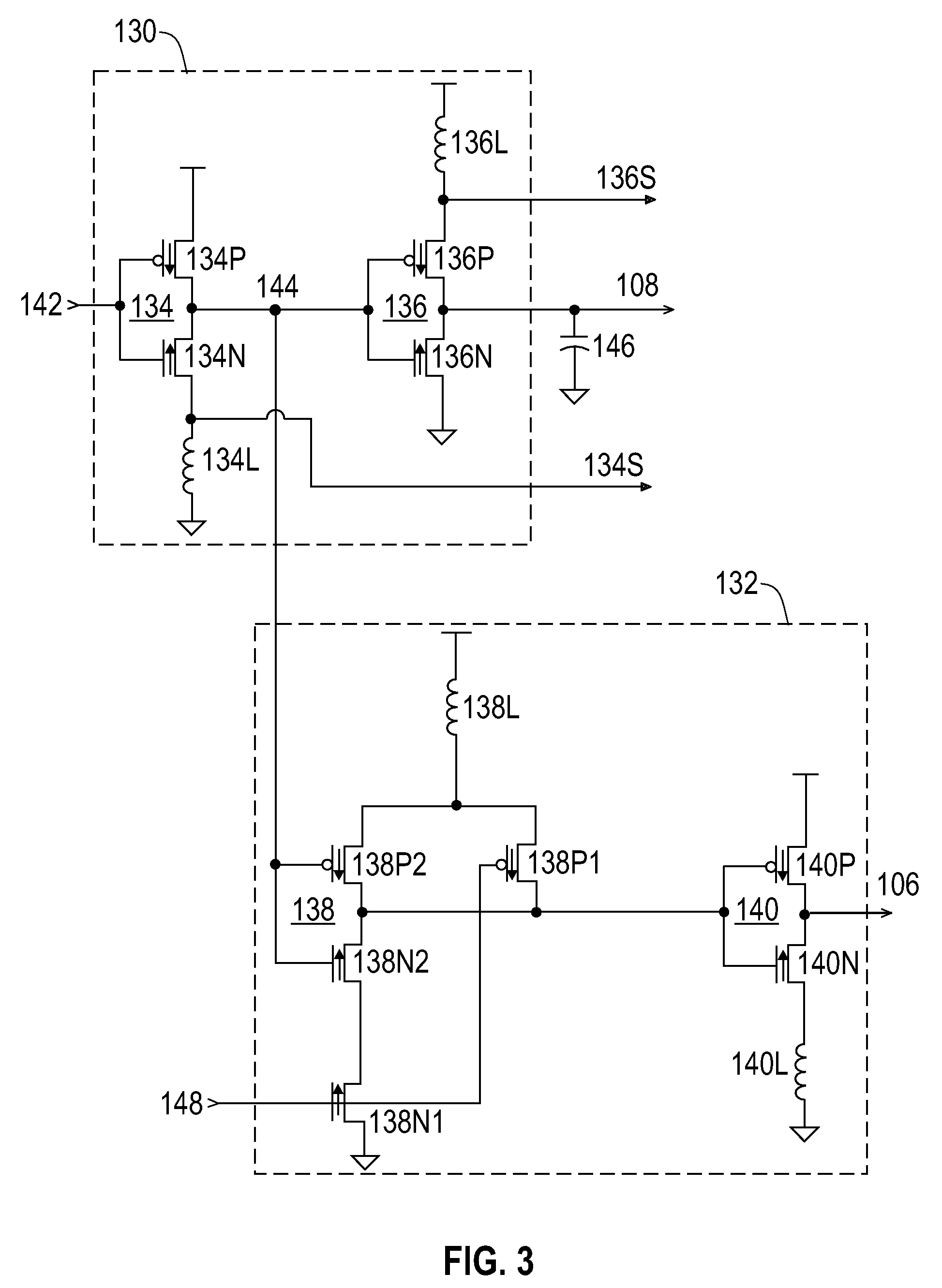
[0013]The present invention relates to a Local Clock Buffer (LCB), an IC chip including registers, some of which may include master / slave latches, locally clocked by the LCB, e.g., providing a launch clock and a capture clock each with an identified critical edge. The LCB includes asymmetrically inductively peaked series connected logic gates (e.g., inverters and / or NAND gates), each with an inductor between gate devices and supply (Vdd) or ground. The series connected gates alternate between having the inductor located between gate devices and the supply and located between gate devices and ground, providing asymmetric inductive peaking to maintain the sharpness of the critical edges. Optionally, corresponding logic gates in multiple LCBs may share the same inductor. Asymmetric inductive peaking allows reducing LCB power without degrading performance.

Problems solved by technology

Thus, not withstanding the decrease of chip supply voltage, chip power consumption has increased as well.
Chip and system level cooling and packaging costs have escalated as a natural result of this increase in chip power.
Consequently, reducing LCB power, a primary contributor to chip power consumption, significantly reduces total chip power.
However, detuning also causes shallower, less well defined clock edges that result in greater timing uncertainty due to the slower edges.
So, where these shallower clock edges are unacceptable (primarily from less current driving a capacitor load and secondarily from driving the LCBs with shallower edges which also contributes to greater timing uncertainty than faster edges), reduced drive current is not a viable solution.

Method used


Image

  • Local clock buffer (LCB) with asymmetric inductive peaking
  • Local clock buffer (LCB) with asymmetric inductive peaking
  • Local clock buffer (LCB) with asymmetric inductive peaking

Examples


Embodiment Construction

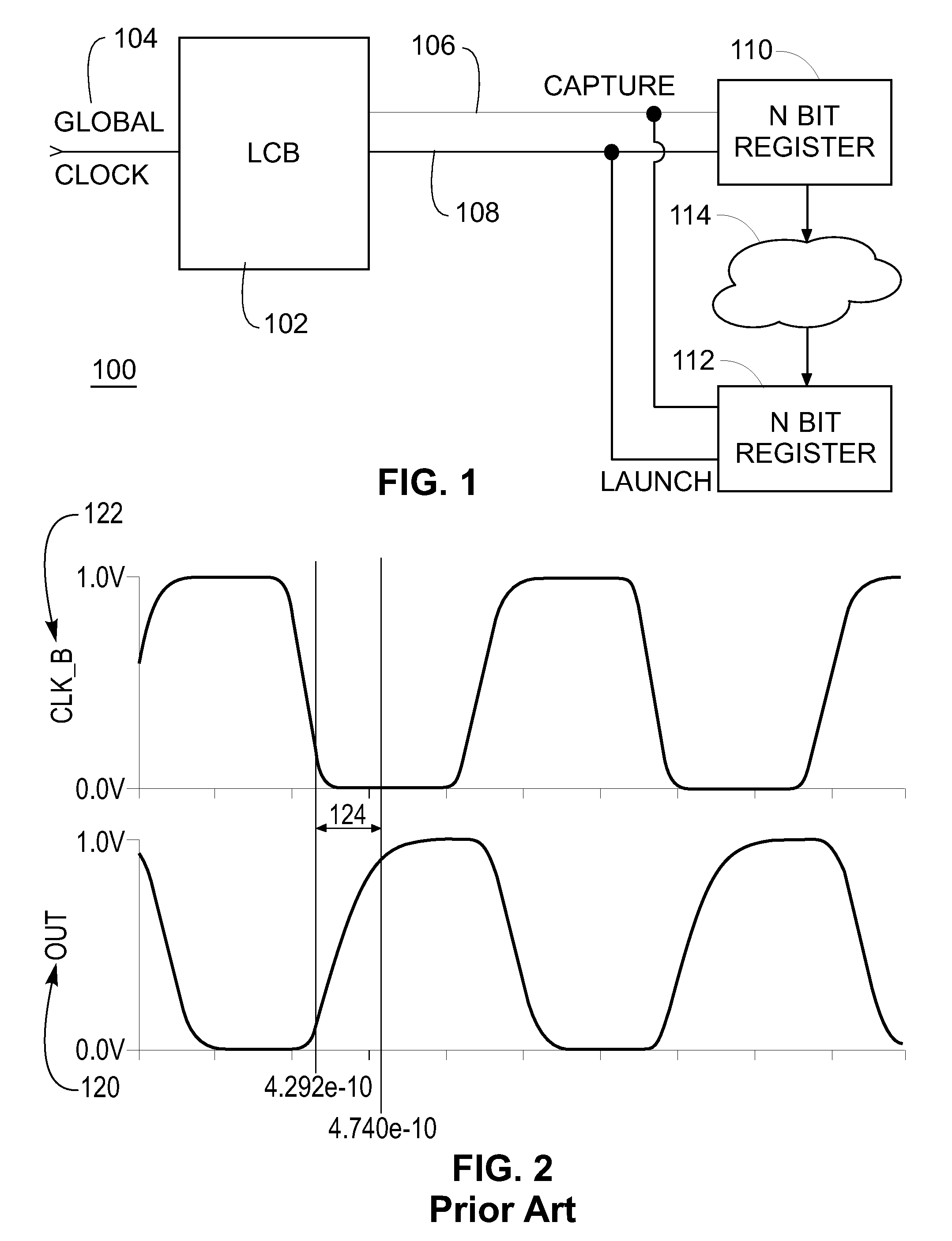
[0021]Turning now to the drawings and, more particularly, FIG. 1 shows a block diagram of an example of clocked pipeline logic 100, clocked by a local clock block (LCB) or clock buffer 102, asymmetrically inductively peaked according to a preferred embodiment of the present invention. A preferred LCB 102 receives and redrives a global chip clock 104 into 2 complementary local clocks, a capture clock 106 and a launch clock 108. Both clocks 106, 108 clock N bit registers 110, 112 on either end of logic 114, e.g., an N-bit data path. In this example, the registers 110, 112 are master / slave registers with logic results being latched in the master latches (not shown) by the launch clock and passed (e.g., from stage 110) through logic (e.g., 114) to the next register stage, 112 in this example. It should be noted that although this example shows a single LCB 102 driving both registers 110, 112, typically, an LCB 102 is provided for each register or a sub-portion thereof. Thus, a typical I...


PUM


Abstract

A Local Clock Buffer (LCB), an IC chip including registers, some of which may include master / slave latches, locally clocked by the LCB, e.g., providing a launch clock and a capture clock each with an identified critical edge. The LCB includes asymmetrically inductively peaked series connected logic gates (e.g., inverters and / or NAND gates), each with an inductor between gate devices and supply (Vdd) or ground. The series connected gates alternate between having the inductor located between gate devices and the supply and located between gate devices and ground, providing asymmetric inductive peaking to maintain the sharpness of the critical edges. Optionally, corresponding logic gates in multiple LCBs may share the same inductor. Asymmetric inductive peaking allows reducing LCB power without degrading performance.

Description

BACKGROUND OF THE INVENTION[0001]1. Field of the Invention[0002]The present invention is related to integrated circuit (IC) clock systems and more particularly to optimizing power consumption in synchronous ICs.[0003]2. Background Description[0004]Semiconductor technology and chip manufacturing advances have resulted in a steady increase of on-chip clock frequencies, the number of transistors on a single chip and the die size itself. These increases have been accompanied by a corresponding decrease in chip supply voltage. Generally, the power consumed by a given clocked unit (e.g., latch, register, register file, functional unit and etc.) or clock driver increases linearly with the frequency of switching within the unit. Thus, not withstanding the decrease of chip supply voltage, chip power consumption has increased as well. Chip and system level cooling and packaging costs have escalated as a natural result of this increase in chip power. It is especially crucial for low end system...

Claims


Application Information

Patent Timeline
IPC IPC(8): H03K19/096H03K19/00
CPCH03K19/018521H03K19/018528H03K19/0963
Inventor FRANCH, ROBERT L.
Owner IBM CORP
Learn More