Vertical cavity surface emitting laser and method of manufacturing it

a laser and vertical cavity technology, applied in lasers, semiconductor devices, semiconductor lasers, etc., can solve the problems of difficult manufacturing of such a high-angle inclined substrate, low laser light output, and high cost of high-angle inclined substrates, and achieve easy and inexpensive manufacturing, and easy and inexpensive manufacturing.

Inactive Publication Date: 2008-10-02
SONY CORP
View PDF5 Cites 48 Cited by
  • Summary
  • Abstract
  • Description
  • Claims
  • Application Information

AI Technical Summary

Benefits of technology

[0019]In the first VCSEL of the embodiment of the invention, the pair of grooves is provided with the region opposed to the light emitting region in between. Thereby, the polarization component in the opposing direction of the pair of grooves is subject to light loss, while the polarization component in the direction orthogonal to the opposing direction of the pair of grooves is hardly subject to light loss. Further, in the embodiment of the invention, the first oxidation region is provided on each side face of the pair of grooves. That is, the first oxidation region is distributed in the opposing direction of the pair of grooves centering on the region opposed to the light emitting region. Therefore, a tension strain is generated in the opposing direction of the pair of grooves in the region opposed to the light emitting region of the first oxidation layer. Thereby, a tension stress according to the magnitude of the tension strain is given to the light emitting region. In the result, the polarization component in the direction orthogonal to the tension stress direction (direction orthogonal to the opposing direction of the pair of grooves) is intensified. Meanwhile, the polarization component in the direction parallel to the tension stress direction (opposing direction of the pair of grooves) is suppressed. Consequently, in the embodiment of the invention, due to two actions by the pair of grooves and the first oxidation region, the polarization component of laser light is fixed in one direction (direction orthogonal to the opposing direction of the pair of grooves). The substrate is not necessarily a special substrate such as an (n11) plane substrate (n is an integer number), but may be a (011) plane substrate.
[0030]As described above, according to the first to the third VCSELs and the method of manufacturing a VCSEL of the embodiments of the invention, the laser is manufactured easily and inexpensively, and the polarization direction of laser light is stabilized in one direction.

Problems solved by technology

Therefore, the high-angle inclined substrate is greatly expensive compared to standard substrates such as a (001) plane substrate.
Therefore, it is difficult to manufacture such a high-angle inclined substrate.
Further, since the output of laser light is low, about 1 mW, which is not a practical output as a light source for a digital copy machine or a printer.
Furthermore, if laser light is emitted from the substrate side, it is necessary to etch the GaAs substrate to the vicinity of a DBR layer to suppress laser absorption by the GaAs substrate, and thus the manufacturing steps become complicated.
Moreover, since the diameter of the mesa is small, there is a possibility that the mesa is broken in the manufacturing process, and thus it is not easy to manufacture the device stably.
However, the polarization direction may not be stabilized in one direction unless the width of the short side of the resonance region is reduced down to the degree at which diffraction loss effects are generated.
Further, assuming that such stabilization of the polarization direction is an effect resulting from a stress or strain due to forming the groove, there is a possibility of an affect of a stress from other factors applied to the device in the crystal growth and a formation process.
As described above, in the related art, it has been difficult to easily manufacture a VCSEL device capable of stabilizing the polarization direction of laser light in one direction.

Method used


Image

  • Vertical cavity surface emitting laser and method of manufacturing it
  • Vertical cavity surface emitting laser and method of manufacturing it
  • Vertical cavity surface emitting laser and method of manufacturing it

Examples


Embodiment Construction

[0050]Descriptions will be given of an embodiment of the invention in detail with reference to the drawings.

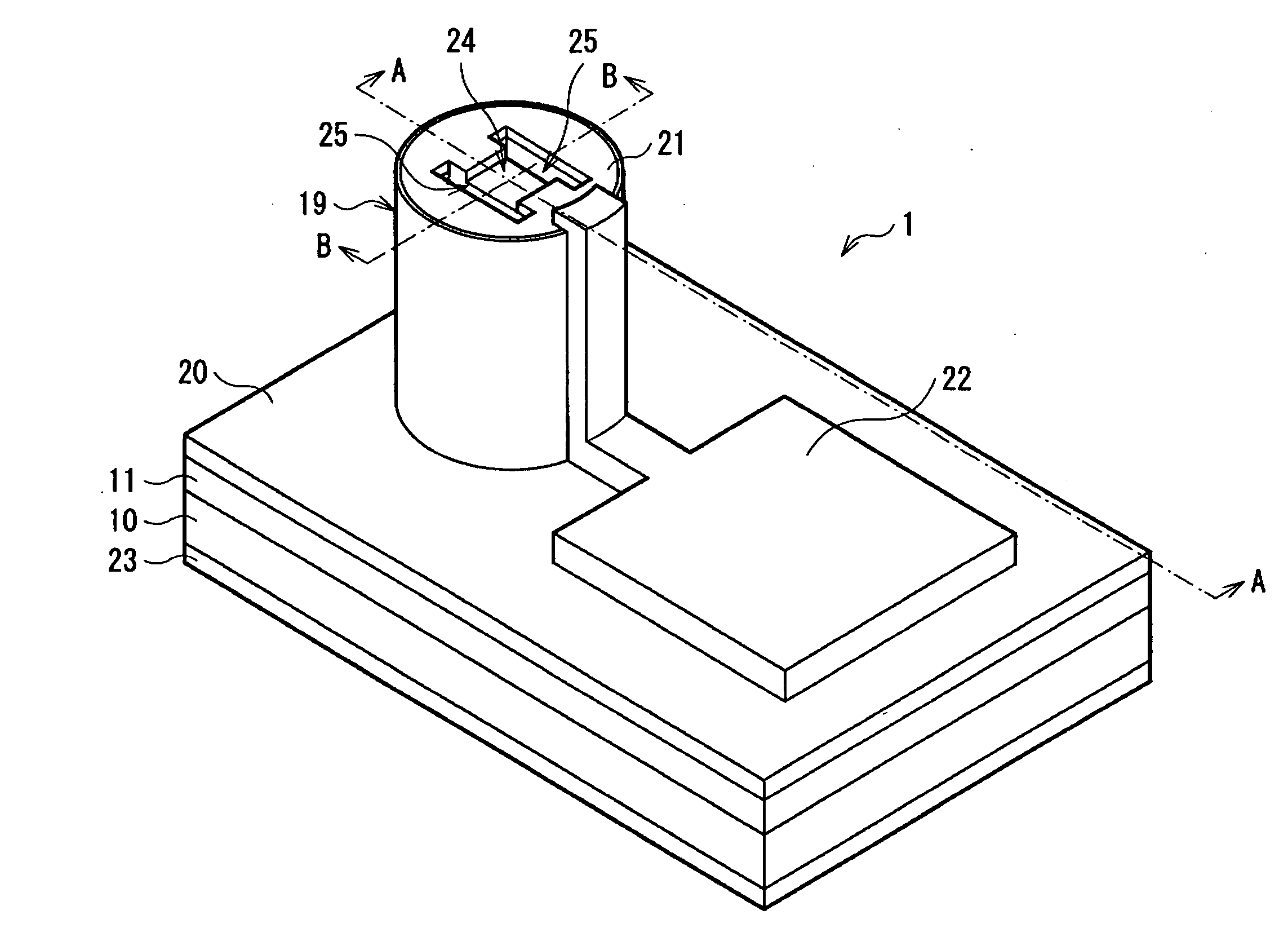
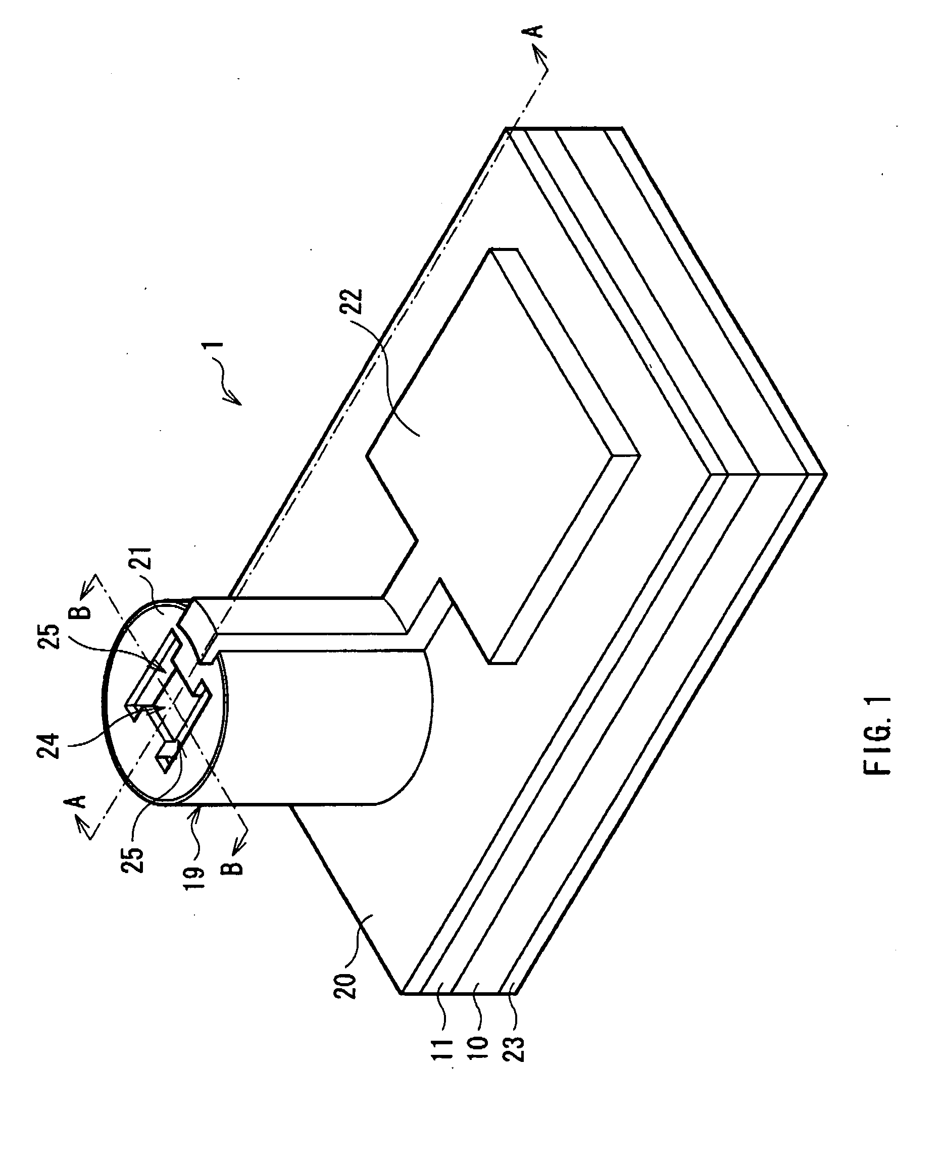
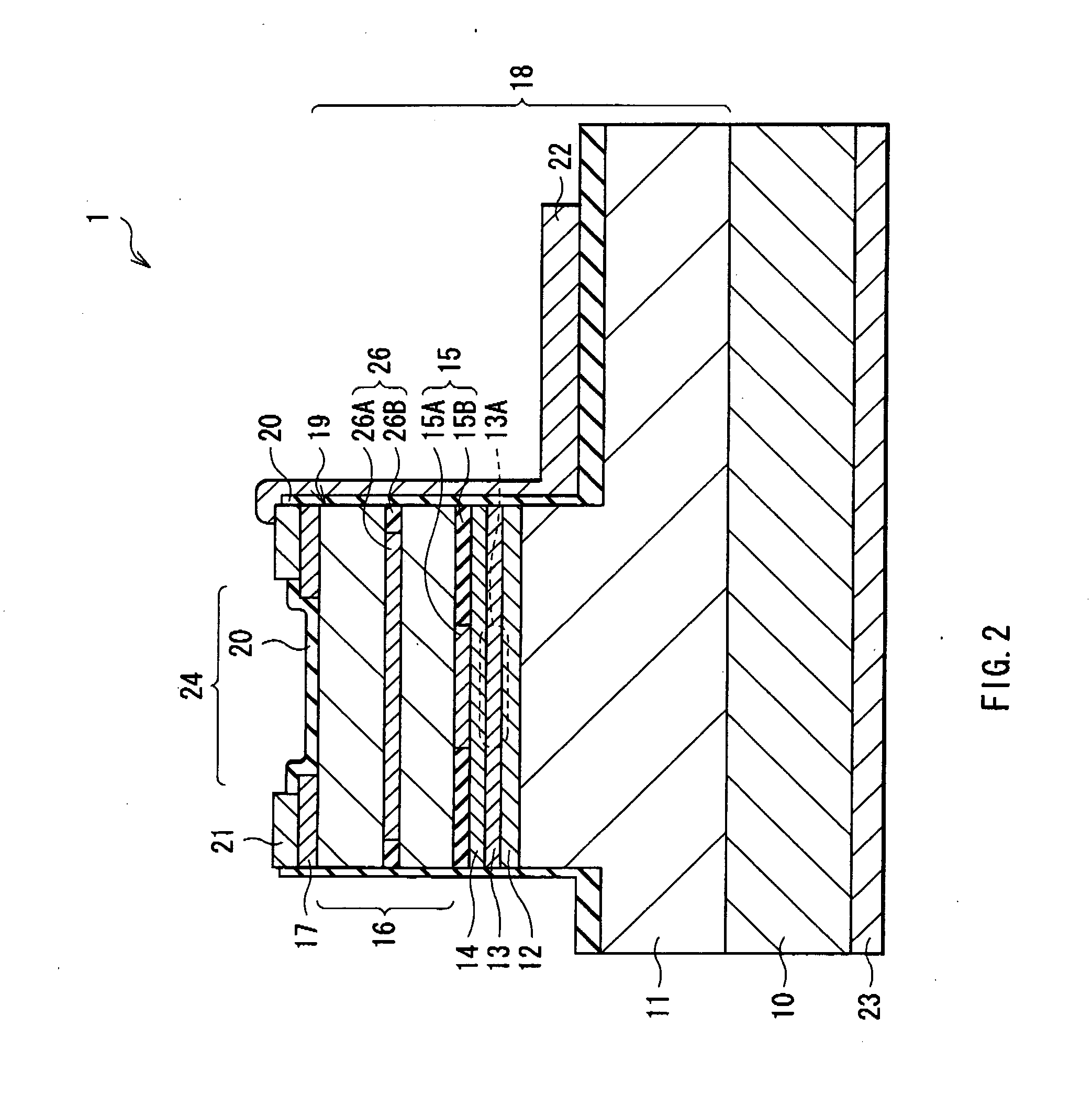
[0051]FIG. 1 shows a perspective view of a VCSEL 1 according to an embodiment of the invention. FIG. 2 shows a cross sectional structure taken along arrows A-A of the VCSEL 1 of FIG. 1. FIG. 3 shows a cross sectional structure taken along arrows B-B of the VCSEL 1 of FIG. 1. FIG. 4 shows a cross sectional structure in a lamination plane of a current confinement layer 15 of FIG. 2 and FIG. 3. FIG. 5 shows an example of a top face structure of a mesa 19 of FIG. 1. FIG. 6 shows another example of a top face structure of the mesa 19 of FIG. 1. FIG. 1 to FIG. 6 are schematic views, and thus the dimensions and the shapes thereof are different from the actual dimensions and the actual shapes.

[0052]The VCSEL 1 has a semiconductor lamination structure 18 in which, for example, a lower DBR mirror layer 11 (first multilayer film reflector), a lower cladding layer 12, an active layer 13, ...


PUM


Abstract

A VSCEL capable of being easily and inexpensively manufactured and of stabilizing the polarization direction of laser light in one direction is provided. The Vertical Cavity Surface Emitting Laser includes a semiconductor lamination structure including a first multilayer film reflector, an active layer having a light emitting region, and a second multilayer film reflector in this order over a substrate from the substrate side. The semiconductor lamination structure has a pair of grooves provided with a region opposed to the light emitting region in between, and one or a plurality of first oxidation layers including a first non-oxidation region provided at least in a region opposed to the light emitting region and a first oxidation region provided on each side face of the pair of grooves.

Description

CROSS REFERENCES TO RELATED APPLICATIONS[0001]The present invention contains subject matter related to Japanese Patent Application JP 2007-081153 filed in the Japanese Patent Office on Mar. 27, 2007, the entire contents of which being incorporated herein by reference.BACKGROUND OF THE INVENTION[0002]1. Field of the Invention[0003]The present invention relates to a Vertical Cavity Surface Emitting Laser (VCSEL) that emits a laser light from the top face and a method of manufacturing it.[0004]2. Description of the Related Art[0005]A VCSEL emits light in the direction orthogonal to a substrate differently from the existing edge-emitting laser diodes. In the VCSEL, many devices can be arranged in a state of a two-dimensional array on the same substrate. Therefore, the VCSEL has recently attracted attention as a light source for a digital copy machine or a printer.[0006]In the past, in the foregoing type of VCSEL, a pair of multilayer film reflectors is formed over the semiconductor subs...

Claims


Application Information

Patent Timeline
Patent Type & Authority Applications(United States)
IPC IPC(8): H01S5/183H01L33/00
CPCH01S5/0425H01S5/1017H01S5/18311H01S5/18313H01S5/18333H01S5/18355H01S5/18391H01S2301/14H01S5/04254
Inventor MAEDA, OSAMUSHIOZAKI, MASAKIYAMAGUCHI, NORIHIKOYAMAUCHI, YOSHINORIARAKIDA, TAKAHIRO
Owner SONY CORP
Why Eureka
Try Eureka