

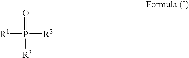
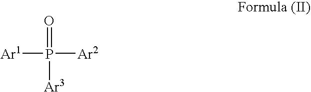
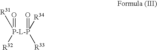
Organic electroluminescence element
a technology of electroluminescence element and organic material, which is applied in the field of organic electroluminescence element, can solve the problems of brightness degradation, low durability, and improvement in light-emission efficiency and drive durability, and achieve excellent drive durability and high light-emission efficiency.
- Summary
- Abstract
- Description
- Claims
- Application Information
AI Technical Summary
Benefits of technology
Problems solved by technology
Method used
Image

Examples
example 1
Preparation of Organic EL Element
1) Formation of Anode
[0164]A product (by Tokyo Sanyo Vacuum Industries Co., Ltd.) manufactured by depositing indium tin oxide (hereinafter, referred to as “ITO”) in a thickness of 150 nm to form a film on a 25 mm×25 mm×0.7 mm glass substrate was used as a transparent substrate. The transparent substrate was subjected to etching and washing.
2) Hole Injection / Transport Layer
[0165]On the ITO glass substrate, 4,4-bis(N-(m-tolyl)-N-phenyl-amino)-biphenyl (hereinafter, referred to as “TPD”) was deposited to give a thickness of 50 nm.
3) Light-Emitting Layer
[0166]On the hole injection / transport layer, a light-emitting layer containing 4,4′-di-(N-carbazole)-biphenyl (hereinafter, referred to as “CBP”) as a host material and fac-tris-(2-phenylpyridinate-N,C2′) iridium (III) (hereinafter, referred to as “Ir(ppy)3”) as a light-emitting material was deposited to give a thickness of 50 nm, wherein the amount of Ir(ppy)3 was 6% by weight with respect to that of CBP...
example 2
Preparation of Organic EL Element
1) Formation of Anode
[0197]A 25 mm×25 mm×0.7 mm glass substrate, on which ITO was deposited with a thickness of 150 nm (manufactured by Tokyo Sanyo Vacuum Industries Co., Ltd.) was used as a transparent substrate. The transparent substrate was subjected to etching and washing.
[0198]On this ITO glass substrate, 4,4′,4′-tris(2-naphthylphenylamino)-triphenylamine (which is referred to hereinafter as 2-TNATA in some cases) was so deposited as to obtain a film thickness of 120 nm.
[0199]On the hole injection layer, N,N′-di-naphthyl-N,N′-diphenyl-[1,1′-biphenyl]-4,4′-diamine (which is referred to hereinafter as α-NPD in some cases) was so deposited as to obtain a film thickness of 10 nm.
4) Light-Emitting Layer
[0200]On the hole transport layer, 1,3-bis(N-carbazolyl)benzene (which is referred to hereinafter as mCP in some cases) as a host material and iridium (III)-bis-(4,6-(di-fluorophenyl)-pyridinate-N, C2′) pic...
example 3
Preparation of Organic EL Element
1) Formation of Anode
[0231]A 25 mm×25 mm×0.7 mm glass substrate, on which ITO was deposited with a thickness of 150 nm (manufactured by Tokyo Sanyo Vacuum Industries Co., Ltd.) was used as a transparent substrate. The transparent substrate was subjected to etching and washing.
[0232]On the ITO glass substrate, 2-TNATA was so deposited as to obtain a film thickness of 120 nm.
[0233]On the hole injection layer, α-NPD was so deposited as to obtain a film thickness of 10 nm.
4) Light-Emitting Layer
[0234]On the hole transport layer, mCP as a host material and platinum complex Pt-1 as a light-emitting material were co-deposited, wherein an amount of Pt-1 was 15% by weight with respect to that of mCP. The thickness was 30 nm.
[0235]On the Light-emitting layer, phosphine oxide compound A-3 was deposited to give a thickness of 40 nm.
6) Electron Injection Layer
[0236]Further, LiF was deposited...
PUM
| Property | Measurement | Unit |
|---|---|---|
| thickness | aaaaa | aaaaa |
| thickness | aaaaa | aaaaa |
| thickness | aaaaa | aaaaa |
Abstract
Description
Claims
Application Information