Method for laying out decoupling cells and apparatus for laying out decoupling cells

a technology of decoupling cells and apparatus, applied in the field of methods and apparatus for laying out decoupling cells (capacitors), can solve problems such as power supply voltage fluctuations, operation errors, and unsuitability for high-integrated semiconductor devices

Inactive Publication Date: 2008-10-02
SOCIONEXT INC
View PDF1 Cites 9 Cited by
  • Summary
  • Abstract
  • Description
  • Claims
  • Application Information

AI Technical Summary

Problems solved by technology

Such simultaneous operation may cause fluctuation in the power supply voltage in a semiconductor device.
Furthermore, operation errors may be caused by power supply noise or timing deviations.
However, the criterion is unclear for the determination of the amount of noise with respect to the positions for laying out the decoupling

Method used


Image

  • Method for laying out decoupling cells and apparatus for laying out decoupling cells
  • Method for laying out decoupling cells and apparatus for laying out decoupling cells
  • Method for laying out decoupling cells and apparatus for laying out decoupling cells

Examples


Embodiment Construction

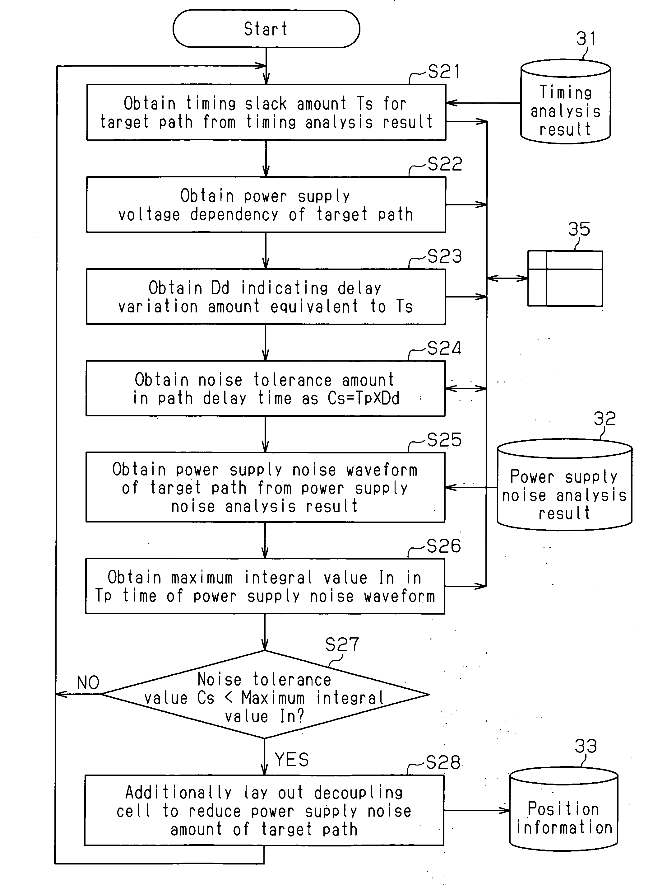
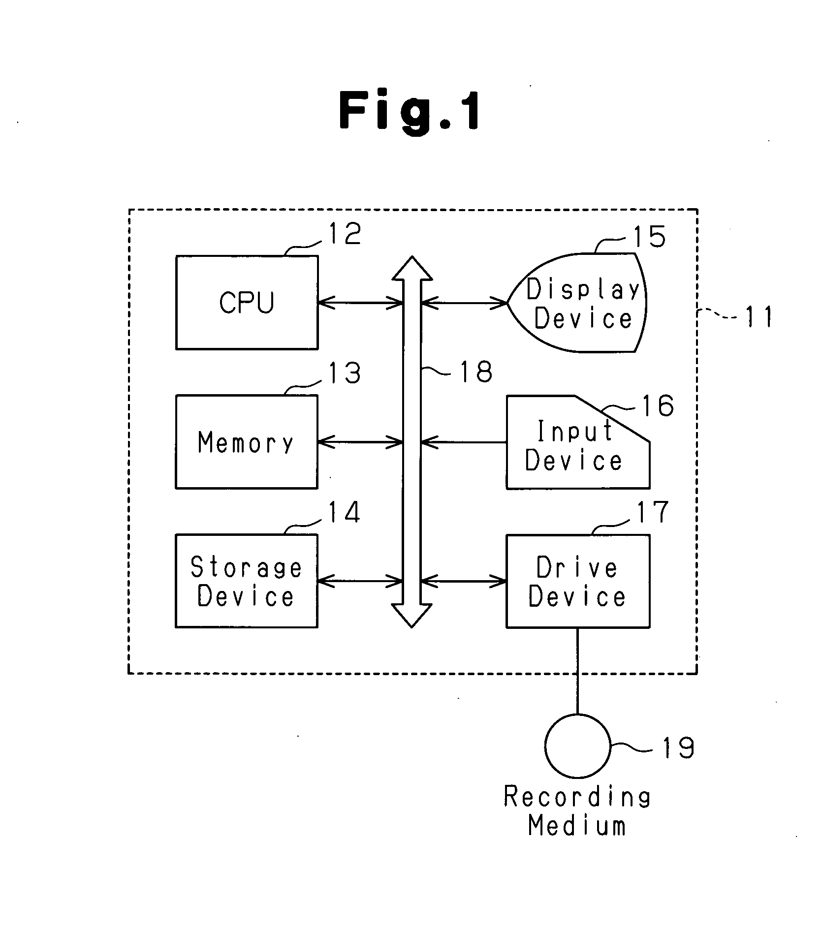
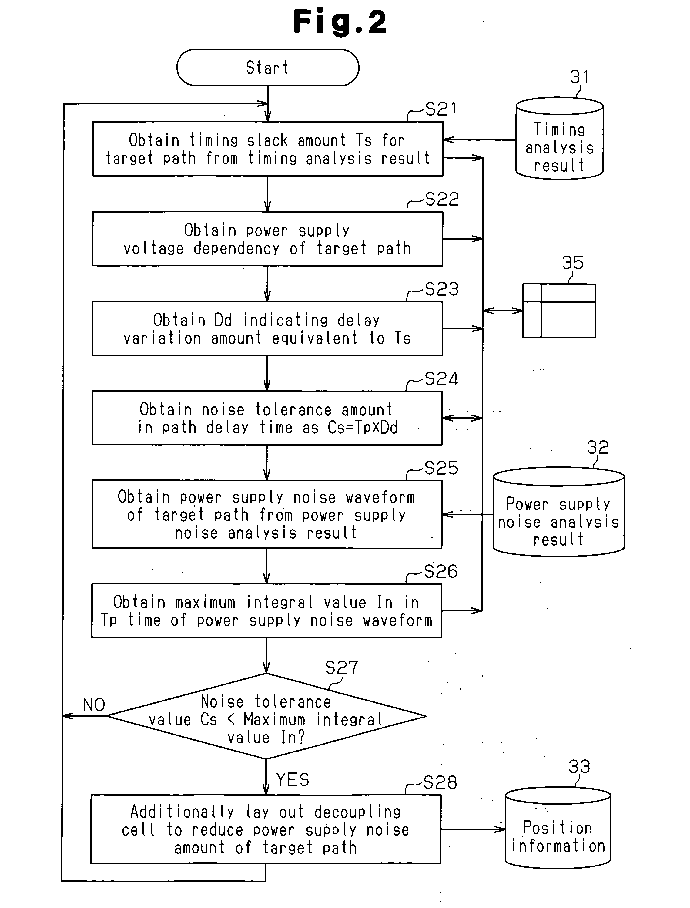
[0019]FIG. 1 shows a decoupling cell layout apparatus 11. The decoupling cell layout apparatus 11 is a typical computer aided design (CAD) apparatus provided with a central processing unit (hereinafter referred to as the “CPU”) 12, a memory 13, a storage device 14, a display device 15, an input device 16, and a drive device 17, which are connected to one another by a bus 18.

[0020]The CPU 12 executes programs with the memory 13 to perform the processing required to lay out decoupling cells. The memory 13 stores programs and data required for laying out decoupling cells. The memory 13 may be a cache memory, a system memory, a display memory, or the like (not shown).

[0021]The display device 15 displays a layout screen and a parameter input screen. The display device 15 may be a CRT, LCD, a PDP, or the like (not shown). The input device 16 includes a keyboard and mouse device (not shown) used to input user requests, instructions, and parameters.

[0022]The storage device 14 may be a magne...


PUM


Abstract

A method for laying out decoupling cells in a semiconductor integrated circuit including a plurality of paths. The method includes extracting from a timing analysis result a timing slack amount as a timing margin for power supply noise in one of the paths serving as a target path, converting the extracted timing margin to a noise tolerance amount, comparing the noise tolerance amount and a power supply noise amount of the target path, and determining whether or not a decoupling cell must be additionally laid out in the target path based on the comparison result.

Description

CROSS-REFERENCE TO RELATED APPLICATIONS[0001]This application is based upon and claims the benefit of priority from the prior Japanese Patent Application No. 2007-090496, filed on Mar. 30, 2007, the entire contents of which are incorporated herein by reference.BACKGROUND[0002]1. Field[0003]The present disclosure relates to a method and apparatus for laying out decoupling cells (capacitors) in a semiconductor device.[0004]2. Description of the Related Art[0005]The enlargement of semiconductor devices has resulted in an increase in the number of simultaneously operated elements. Such simultaneous operation may cause fluctuation in the power supply voltage in a semiconductor device. Furthermore, operation errors may be caused by power supply noise or timing deviations. Therefore, to reduce power supply noise, decoupling cells (capacitors) are laid out between a low-voltage power supply wiring and a high-voltage power supply wiring of a semiconductor device. In a semiconductor device pr...

Claims


Application Information

Patent Timeline
IPC IPC(8): G06F17/50
CPCG06F17/5031G06F2217/78G06F30/3312G06F2119/06
Inventor OKUMURA, TAKAAKI
Owner SOCIONEXT INC
Why Eureka
Try Eureka