Opto-electronic board

a technology of optoelectronic boards and optical components, applied in the direction of optical elements, circuit optical details, instruments, etc., can solve the problems of increasing the cost of optical boards, increasing the resistance of copper wiring of pwbs, and becoming increasingly difficult to achieve electrically, so as to achieve efficient coupling in and out of waveguides and mechanically better positions

Active Publication Date: 2008-10-09
INT BUSINESS MASCH CORP
View PDF8 Cites 9 Cited by
  • Summary
  • Abstract
  • Description
  • Claims
  • Application Information

AI Technical Summary

Benefits of technology

[0009]According to a first exemplary aspect of the invention there is provided an opto-electronic board with a waveguide and an opto-electronic circuit, wherein the opto-electronic circuit is aligned relative to the waveguide so that the light can be more efficiently coupled in and out of the waveguide. With the help of the invention the opto-electronic circuit can be mechanically better located.
[0010]There may be provided electrical connections between the transmitter or receiver of the electronic signals and the opto-electronic circuit. With this embodiment, the electrical connections can be kept shorter and loss and distortion can be reduced.

Problems solved by technology

As the signal frequencies are now in the 10 GHz range this is becoming increasingly difficult to accomplish electrically, mainly because of the dielectric losses of the insulating materials in the circuit board.
Even if lower loss dielectric materials can be employed, as frequencies increase further, the resistance of the copper wiring of the PWB will eventually become a limiting factor.
This leads to the problem of mounting the opto-electronic converters relative to the waveguide so that the light can be efficiently coupled in and out of the waveguide.
The realization of mirrors in the waveguide layer is a specialized process that increases the cost of the optical board.
This approach avoids the use of mirrors but requires edge emitting lasers, which are generally more expensive than surface emitting lasers.
Furthermore, edge receiving detectors are not available as standard components.

Method used


Image

  • Opto-electronic board
  • Opto-electronic board
  • Opto-electronic board

Examples


Embodiment Construction

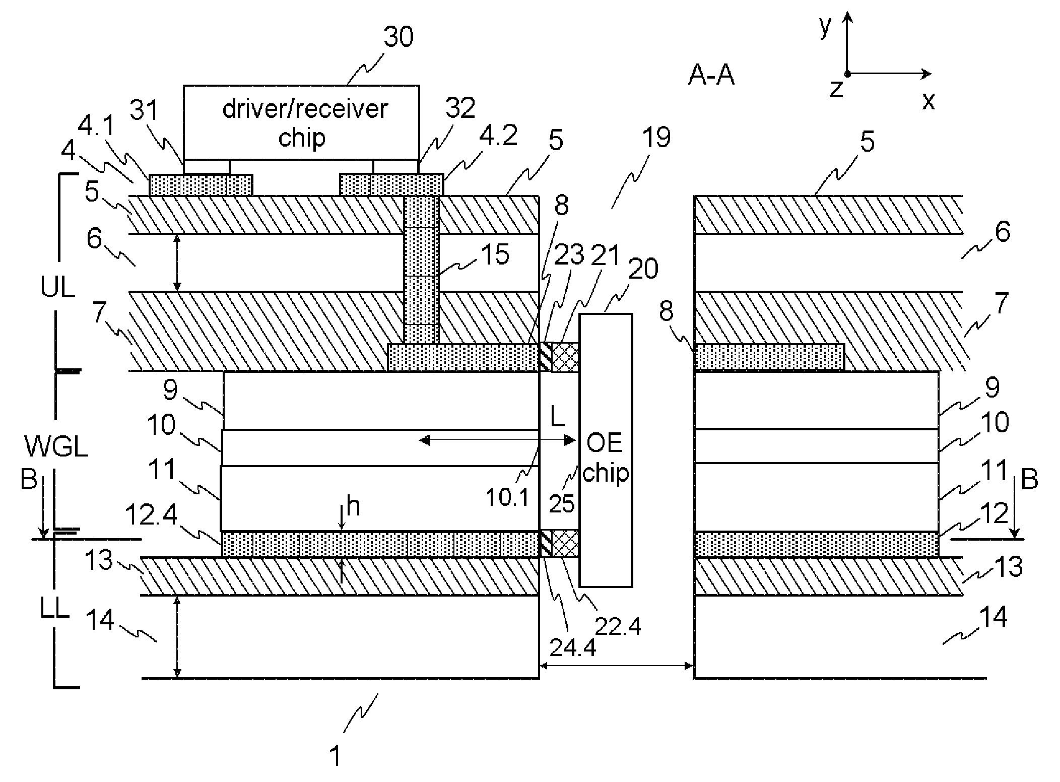
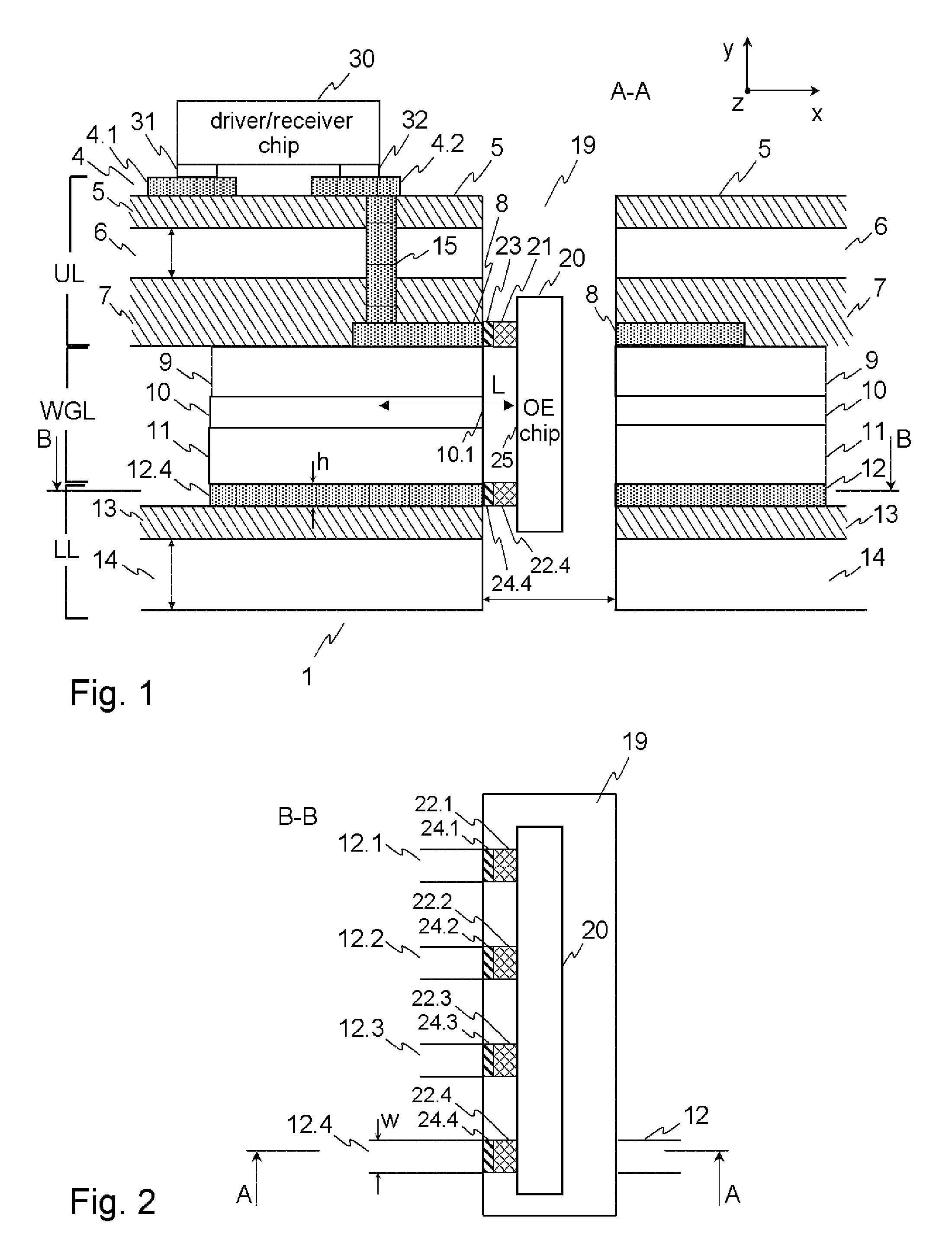
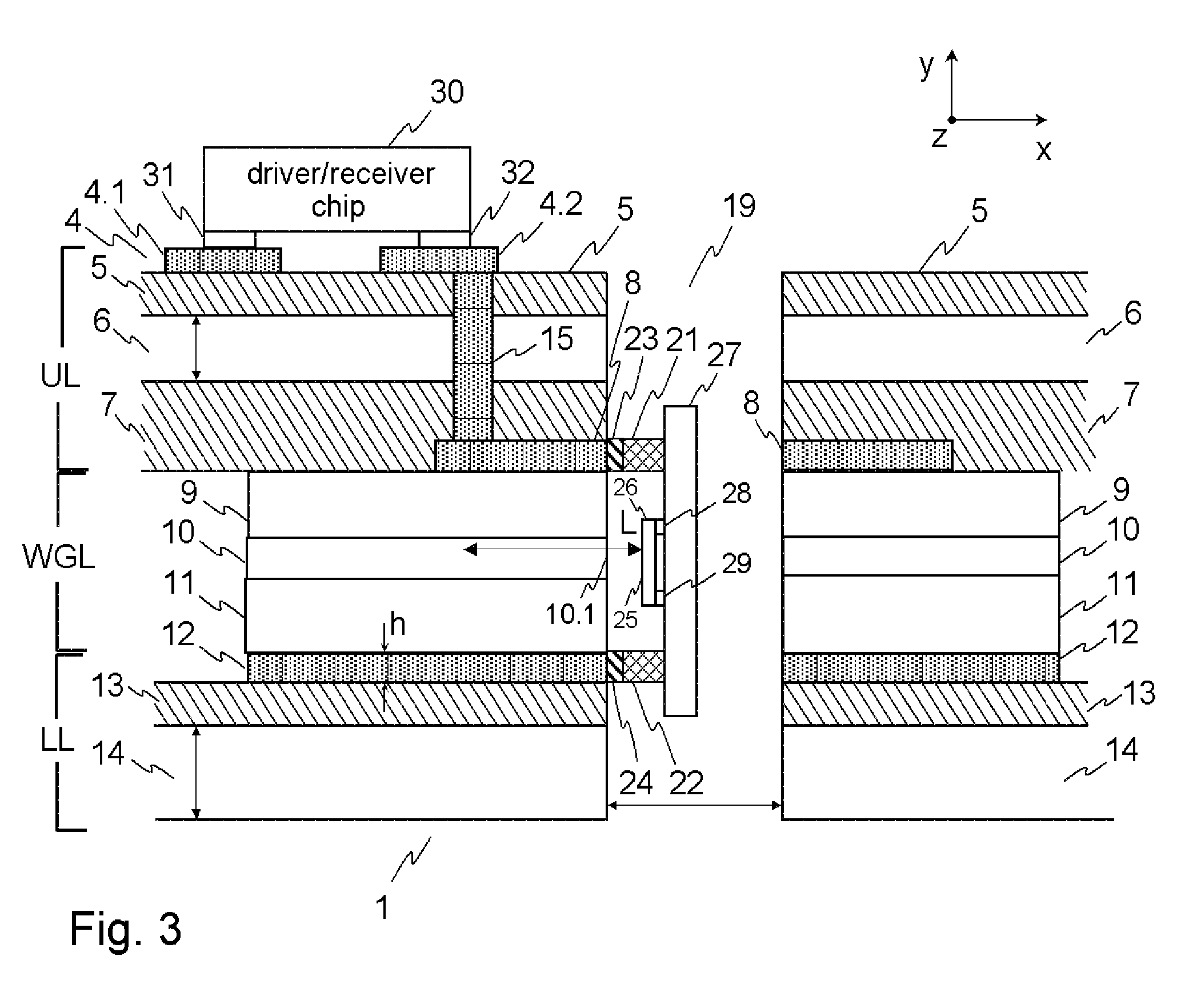
[0027]FIG. 1 illustrates a first embodiment of the opto-electronic board with a printed wiring board 1 in cross section. The intersection runs along the intersecting line A-A which is depicted in FIG. 2. FIG. 2 illustrates a clipper of the opto-electronic board 1 in longitudinal section along the intersecting line B-B which is depicted in FIG. 1.

[0028]The printed wiring board 1 is equipped with two chips. One of the two chips is a driver / receiver chip 30 which is mounted on top of the printed wiring board 1. The driver / receiver chip 30 has bonding pads soldered to wiring tracks of the printed wiring board 1. In FIG. 1 two of the bonding pads, indicated with the reference signs 31 and 32, are depicted. The second chip is an opto-electrical circuit 20, which is mounted in a hole 19 of the printed wiring board 1. The expressions opto-electrical circuit, opto-electrical (O / E) converter chip, electro-optical (E / O) converter chip, or shortly converter chip are used in the following as syn...


PUM


Abstract

An opto-electronic board including a printed wiring board with an optical waveguide, a metallic area, and a hole, wherein an abutting face of the optical waveguide and an abutting face of the metallic area form a part of the side face of the hole. The opto-electronic board further comprises an opto-electronic circuit with a bonding pad, wherein the opto-electronic circuit is arranged in the hole and soldered with its bonding pad to the abutting face of the metallic area.

Description

CROSS-REFERENCE TO RELATED APPLICATIONS[0001]This application claims priority under 35 U.S.C. § 119 to European Patent Application No. 05112948.4 filed Dec. 23, 2005, the entire text of which is specifically incorporated by reference herein.BACKGROUND OF THE INVENTION[0002]The present invention relates to an opto-electronic board and to a method of mounting an opto-electronic circuit on a hybrid printed circuit board. The hybrid printed circuit board comprises an optical waveguide and electrical tracks.[0003]The transmission of high frequency signals over distances of 1 to 3 meters on printed wiring boards (PWB) and through several connectors, with low loss and distortion is desired in several applications such as high-speed servers and routers. As the signal frequencies are now in the 10 GHz range this is becoming increasingly difficult to accomplish electrically, mainly because of the dielectric losses of the insulating materials in the circuit board. Even if lower loss dielectric...

Claims


Application Information

Patent Timeline
Patent Type & Authority Applications(United States)
IPC IPC(8): G02B6/12
CPCG02B6/4232G02B6/4249H05K1/0274H05K1/184H05K2201/10121
Inventor DELLMANN, LAURENT A.DESPONT, MICHELOFFREIN, BERT J.WEBB, DAVID J.
Owner INT BUSINESS MASCH CORP
Why Eureka
Try Eureka