Spring interconnect structures

a technology of interconnection elements and springs, which is applied in the direction of coupling device connections, semiconductor/solid-state device details, instruments, etc., can solve the problems of increasing the difficulty of fabricating interconnections, limiting the design choices for the shape and metallurgy of the contact portion of the interconnection elements, and increasing the difficulty of controlling or establishing desired shapes at the contact end. , to achieve the effect of improving the mechanical properties of each interconnection element, reducing the pitch, and improving the body

Inactive Publication Date: 2008-10-16
FORMFACTOR INC
View PDF67 Cites 8 Cited by
  • Summary
  • Abstract
  • Description
  • Claims
  • Application Information

AI Technical Summary

Benefits of technology

[0025]An electronic component according to the invention is particularly suitable for making temporary or permanent electrical connection with a second electronic component having “fine-pitch” contact pads or terminals, for example, spacing of at least less than 5 mils (130 μm), such as 2.5 mils (65 μm). As will be evident from the description that follows, minimized pitch between interconnection elements of an electronic component of the invention is achieved in part by modifying the thickness of the body or spring portion of the interconnection element of the electronic component. Instead of a single beam body, the interconnection elements of the electronic component are comprised of a plurality of resilient elements to improve the mechanical properties of each interconnection element. A desired spring constant of multiple, coordinated springs reinforce and support the primary spring and interconnection element (e.g., tip). A leaf portion body also improves the compliance of the body at a reduced material stress. Applications to larger scale devices, including, for example, devices with contact pitches of about 50-100 mil (1.3-2.6 mm) and even larger are feasible as well.

Problems solved by technology

With respect to the tungsten needle as a spring interconnection element, for example, the contact end is limited by the metallurgy of the element (i.e., tungsten) and, as the tungsten needle becomes smaller in diameter, it becomes commensurately more difficult to control or establish a desired shape at the contact end.
Again, the technology required to manufacture such interconnection elements limits the design choices for the shape and metallurgy of the contact portion of the interconnection elements.
As electronic components get increasingly smaller and the spacing between terminals on the electronic components get increasingly tighter or the pitch gets increasingly finer, it becomes increasingly more difficult to fabricate interconnections including spring interconnection elements suitable for making electrical connection to terminals of an electronic component.

Method used


Image

  • Spring interconnect structures
  • Spring interconnect structures
  • Spring interconnect structures

Examples


Embodiment Construction

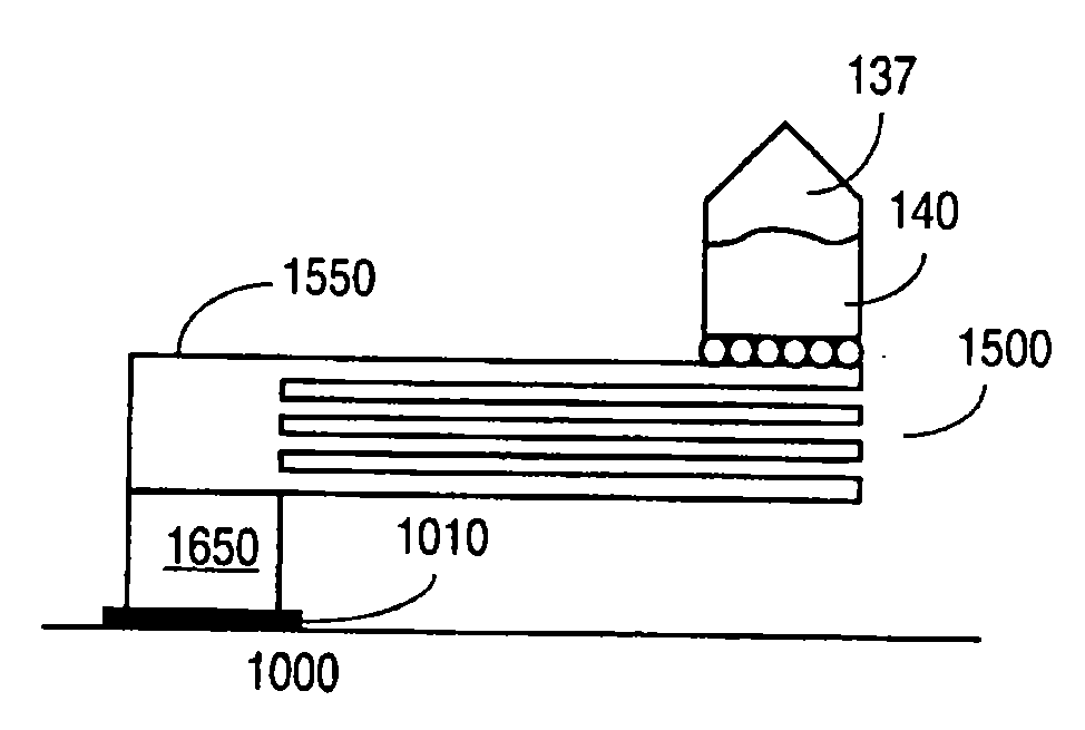
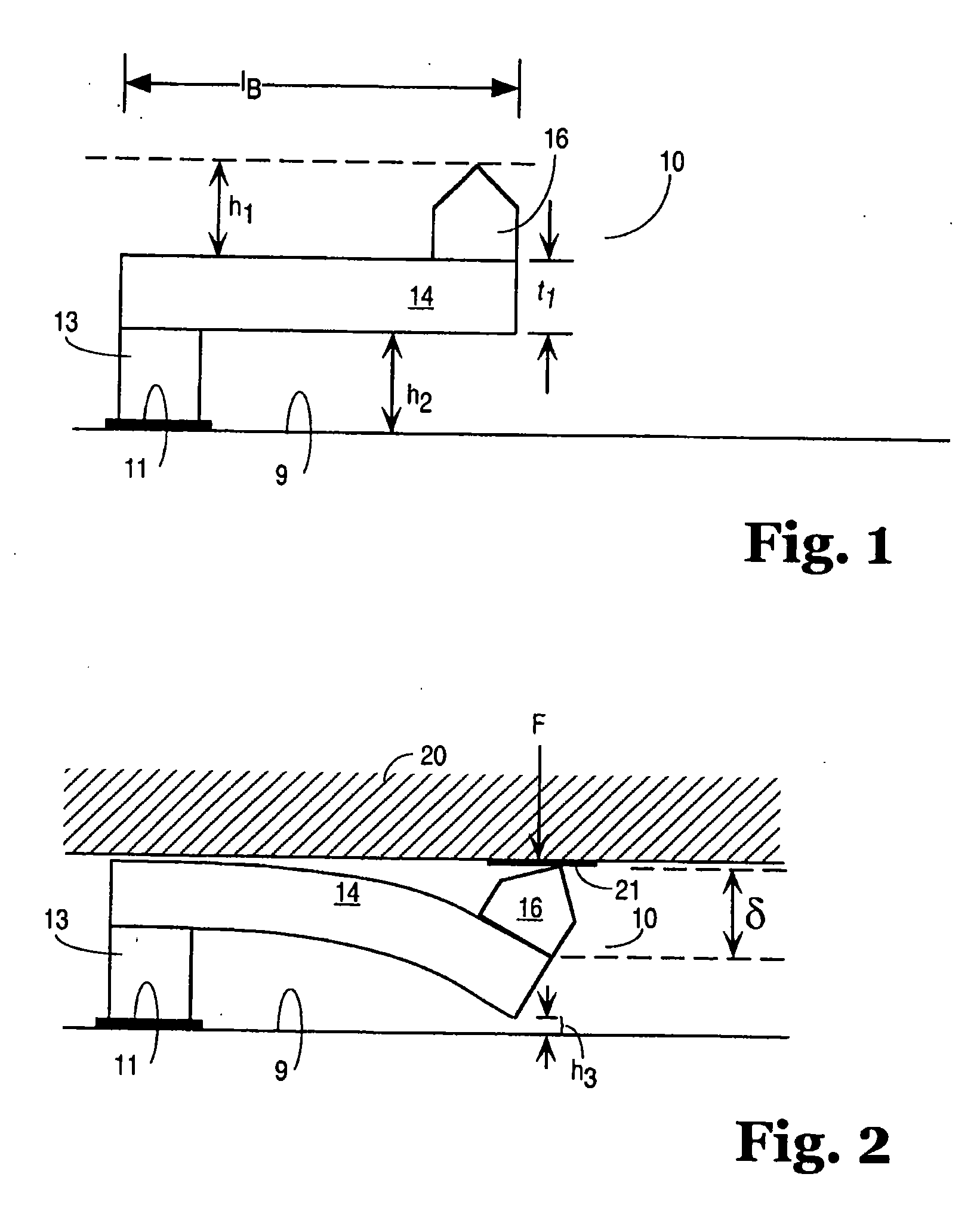
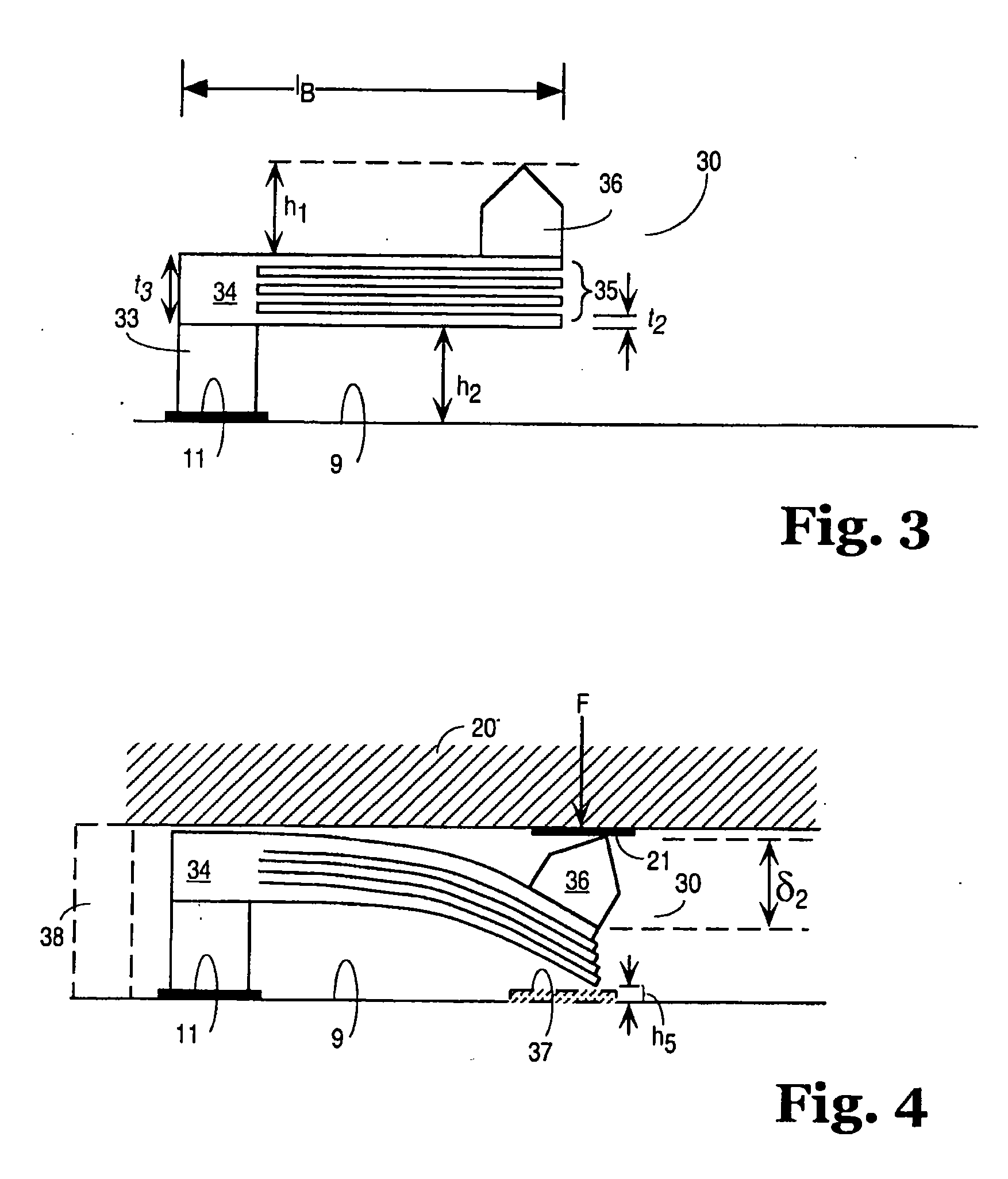
[0119]The invention relates to interconnection elements, including contact elements. According to one aspect of the invention, the invention contemplates a method of forming an interconnection element having a body including a plurality of resilient or flexural elements, e.g., leaf portions. The invention also relates to a method of bringing together two substrates, such as an electronic component having a plurality of interconnection elements with a second electronic component having an array of contact pads or terminals.

[0120]Suitable electronic components include, but are not limited to, an active semiconductor device, a memory chip, a portion of a semiconductor wafer, a ceramic substrate, an organic substrate, a PCB, an organic membrane, a polyimide sheet, a space transformer, a probe card, a chip carrier, and a socket. The electronic component may be an active device or a passive device that supports one or more electronic connections. In general, suitable electronic components...


PUM

PropertyMeasurementUnit
sizeaaaaaaaaaa
pressureaaaaaaaaaa
resilientaaaaaaaaaa

Abstract

An interconnection element of a spring (body) including a first resilient element with a first contact region and a second contact region and a first securing region and a second resilient element, with a third contact region and a second securing region. The second resilient element is coupled to the first resilient element through respective securing regions and positioned such that upon sufficient displacement of the first contact region toward the second resilient element, the second contact region will contact the third contact region. The interconnection, in one aspect, is of a size suitable for directly contacting a semiconductor device. A large substrate with a plurality of such interconnection elements can be used as a wafer-level contactor. The interconnection element, in another aspect, is of a size suitable for contacting a packaged semiconductor device, such as in an LGA package.

Description

RELATED APPLICATIONS[0001]This application is continuation-in-part of patent application Ser. No. 09 / 205,022 filed Dec. 2, 1998 entitled “Lithographic Contact Elements,” and patent application Ser. No. 09 / 205,023 filed Dec. 2, 1998 entitled “Lithographic Contact Elements.”BACKGROUND OF THE INVENTION[0002]1. Field of the Invention[0003]The invention relates to an interconnection (contact) element suitable for effecting pressure connections between electronic components and is particularly useful for contacting semiconductor packages or for contacting a semiconductor directly.[0004]2. Description of Related Art[0005]Interconnection or contact elements may be used to connect devices of an electronic component or one electronic component to another electronic component. For example, an interconnection element may be used to connect two circuits of an integrated circuit chip or including an application specific integrated circuit (ASIC). Interconnection elements may also be used to conne...

Claims


Application Information

Patent Timeline
Patent Type & Authority Applications(United States)
IPC IPC(8): H01R12/00G01R1/073G01B7/34G01N27/00G01R1/067G01R3/00H01L21/48H01L21/60H01L21/66H01L23/48H01R12/16H01R33/76H05K3/32H05K3/40
CPCG01R1/06727G01R1/06761G01R3/00H01L2924/14H05K3/326H01L2924/0002H05K3/4092H01L2924/01005H01L2924/00G01R1/067
Inventor MATHIEU, GAETAN L.ELDRIDGE, BENJAMIN N.GRUBE, GARY W.LARDER, RICHARD A.
Owner FORMFACTOR INC
Why Eureka
Try Eureka