Substrate processing apparatus

a processing apparatus and substrate technology, applied in the direction of chemical vapor deposition coating, electric discharge tubes, coatings, etc., can solve the problems of inability to pass therethrough at a high rate, and inability to rapidly raise the temperature of the mounting stage, etc., to achieve efficient flow of cold gas

Inactive Publication Date: 2008-10-23
TOKYO ELECTRON LTD
View PDF9 Cites 349 Cited by
  • Summary
  • Abstract
  • Description
  • Claims
  • Application Information

AI Technical Summary

Benefits of technology

[0027]With this arrangement, it is possible to efficiently flow the cold gas into the gas inflow chamber. The above and other objects, features,...

Problems solved by technology

This deposit film can cause problems, such as a conduction failure, for electronic devices and hence must be removed.
For this reason, it is not possible to rapidly raise the temperature of the mounting stage, though the temperature can be increased using the heater.
In addition, a coolant made to pass through the coolant channel is a liquid and, therefore, cannot be made to pass therethroug...

Method used


Image

  • Substrate processing apparatus
  • Substrate processing apparatus
  • Substrate processing apparatus

Examples


first embodiment

[0034]First, a description will be made of a substrate processing system having a substrate processing apparatus according to the present invention.

[0035]FIG. 1 is a plan view schematically showing the configuration of a substrate processing system having a substrate processing apparatus according to a present embodiment.

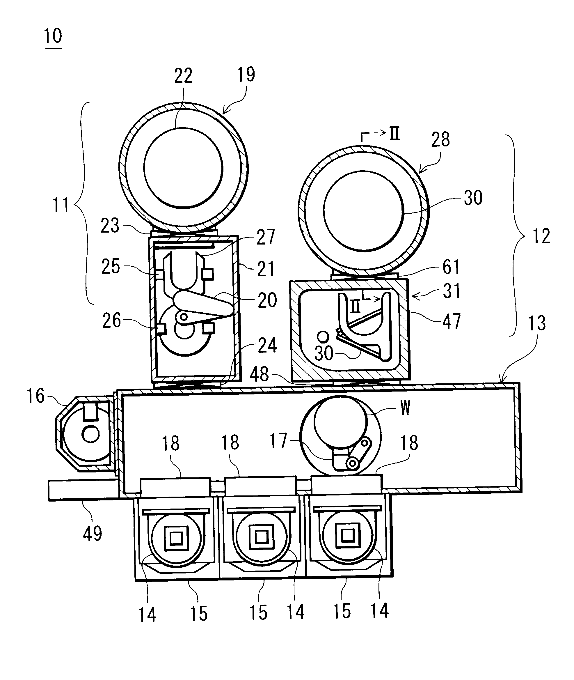
[0036]In FIG. 1, a substrate processing apparatus 10 has a first process ship 11 for performing a plasma processing on a wafer W (substrate) for semiconductor devices (hereinafter simply referred to as the “wafer W”), a second process ship 12 disposed parallel to the first process ship 11 to perform a chemical reaction treatment and a heating treatment on the plasma-treated wafer W, and a loader module 13 provided as a rectangular common transfer chamber to which the first and second process ships 11 and 12 are connected.

[0037]In addition to the first and second process ships 11 and 12, there are connected to the loader module 13 three FOUP mounting stages 15, on ea...

second embodiment

[0067]Next, a description will be made of a substrate processing system having a substrate processing apparatus according to the present invention.

[0068]The present embodiment, which is basically the same in configuration and effect as the first embodiment described above, only differs from the first embodiment in the configuration of the mounting stage of the second process module. Accordingly, like constituent elements will not be explained again and only those constituent elements and effects different from those of the first embodiment will be described hereinafter.

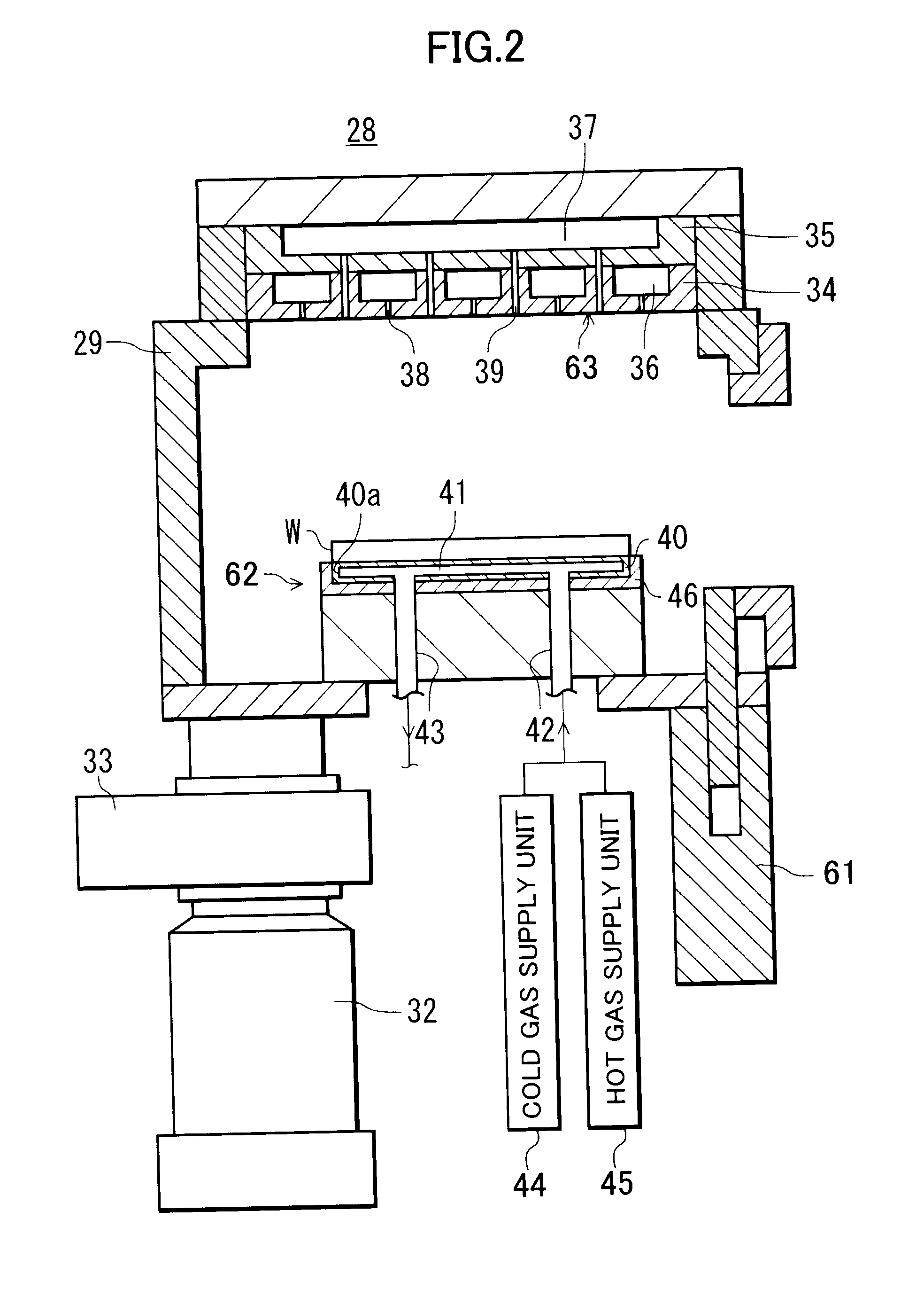
[0069]FIG. 4 is a sectional view of a second process module 50 provided as a substrate processing apparatus according to an embodiment of the present invention.

[0070]In FIG. 4, the second process module 50 (substrate processing apparatus) is disposed within the chamber 29 and has a mounting stage 51 for a wafer W to be mounted on and for controlling the processing temperature of the mounted wafer W.

[0071]A jacket 40 t...


PUM

PropertyMeasurementUnit
Temperatureaaaaaaaaaa
Thicknessaaaaaaaaaa

Abstract

A substrate processing apparatus capable of rapidly raising and lowering the processing temperature of a substrate. The substrate processing apparatus has a mounting stage adapted to be mounted with a substrate and to control the processing temperature of the mounted substrate. The mounting stage comprises a temperature control device disposed in a mounting surface of the mounting stage for mounting the substrate thereon, a coolant inflow chamber into which a coolant is flowed, and a heat transmission/insulation switch-over chamber disposed between the temperature control device and the coolant inflow chamber so that a heat-transmitting gas is flowed into and vacuum-exhausted from the heat transmission/insulation switch-over chamber. The temperature control device has therein a gas inflow chamber into which a hot gas is flowed.

Description

BACKGROUND OF THE INVENTION[0001]1. Field of the Invention[0002]The present invention relates to a substrate processing apparatus, and more particularly, to a substrate processing apparatus having a mounting stage for a substrate to be mounted on and for controlling the processing temperature of the mounted substrate.[0003]2. Description of the Related Art[0004]In a method for manufacturing semiconductor devices from a silicon wafer (hereinafter simply referred to as the “wafer”), there are successively and cyclically carried out a film formation step, such as chemical vapor deposition (CVD), wherein a conductive film or an insulating film is formed on a surface of the wafer; a lithography step wherein desired patterns of a photoresist layer is formed on the conductive film or the insulating film thus formed; and an etching step wherein the conductive film is shaped into gate electrodes or wiring trenches and contact holes are formed in the insulating film by plasma produced from a ...

Claims


Application Information

Patent Timeline
IPC IPC(8): C23F1/02C23C16/52
CPCC23C16/4583C23C16/46C23C16/466H01J37/20H01J2237/2001H01L21/02071H01L21/67109
Inventor HAYASHI, DAISUKENAGASEKI, KAZUYA
Owner TOKYO ELECTRON LTD
Why Eureka
Try Eureka