Electromagnetic bandgap structure and printed circuit board

a bandgap structure and printed circuit board technology, applied in the direction of waveguides, line-transmission details, waveguide type devices, etc., can solve the problems of reducing the size affecting the accuracy of the rf circuit, and the difficulty of accurately receiving the signal ranging a certain frequency band, etc., to achieve the effect of low bandgap frequency band and not increasing the siz

a bandgap structure and printed circuit board technology, applied in the direction of waveguides, line-transmission details, waveguide type devices, etc., can solve the problems of reducing the size affecting the accuracy of the rf circuit, and the difficulty of accurately receiving the signal ranging a certain frequency band, etc., to achieve the effect of low bandgap frequency band and not increasing the siz

US20080266018A1Inactive Publication Date: 2008-10-30SAMSUNG ELECTRO MECHANICS CO LTD

Image

  • Electromagnetic bandgap structure and printed circuit board
  • Electromagnetic bandgap structure and printed circuit board
  • Electromagnetic bandgap structure and printed circuit board

Examples


Embodiment Construction

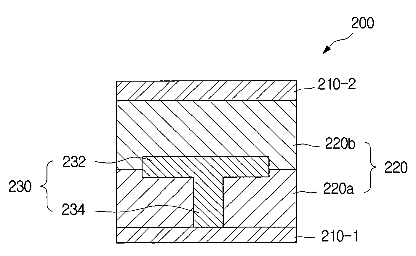
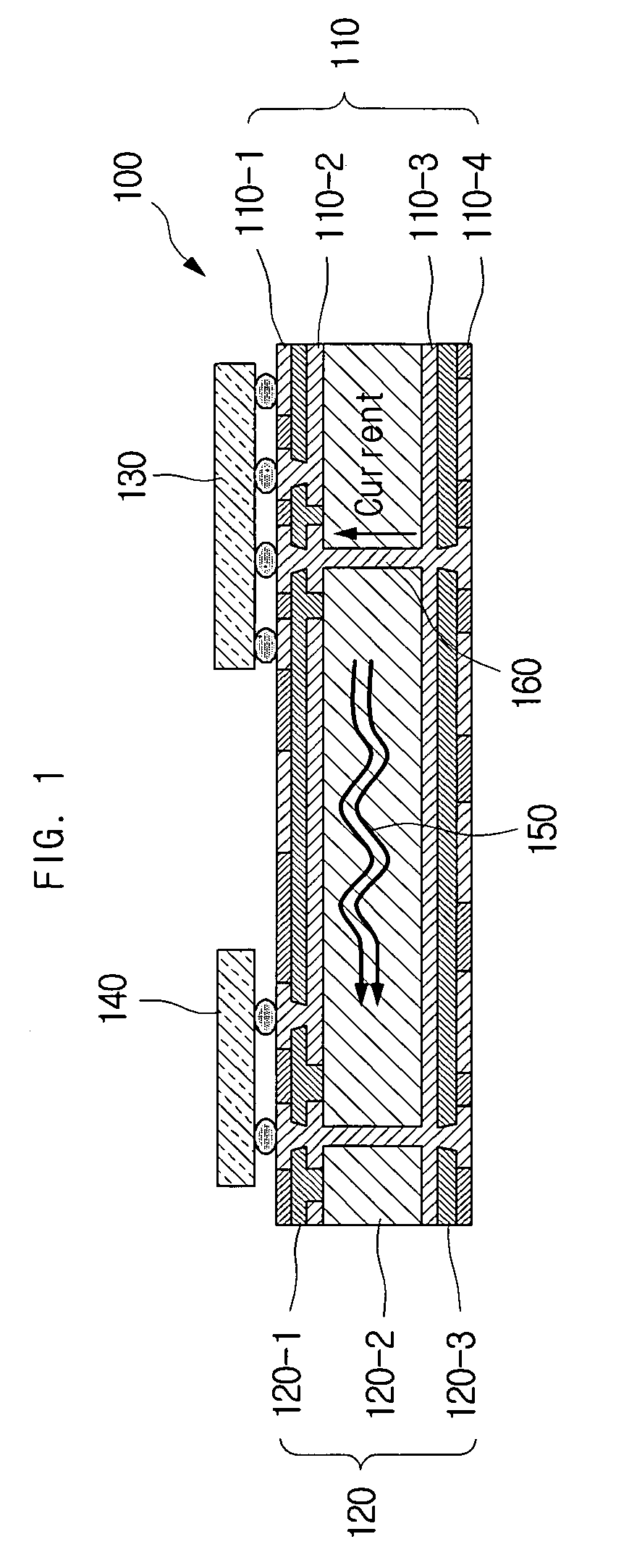
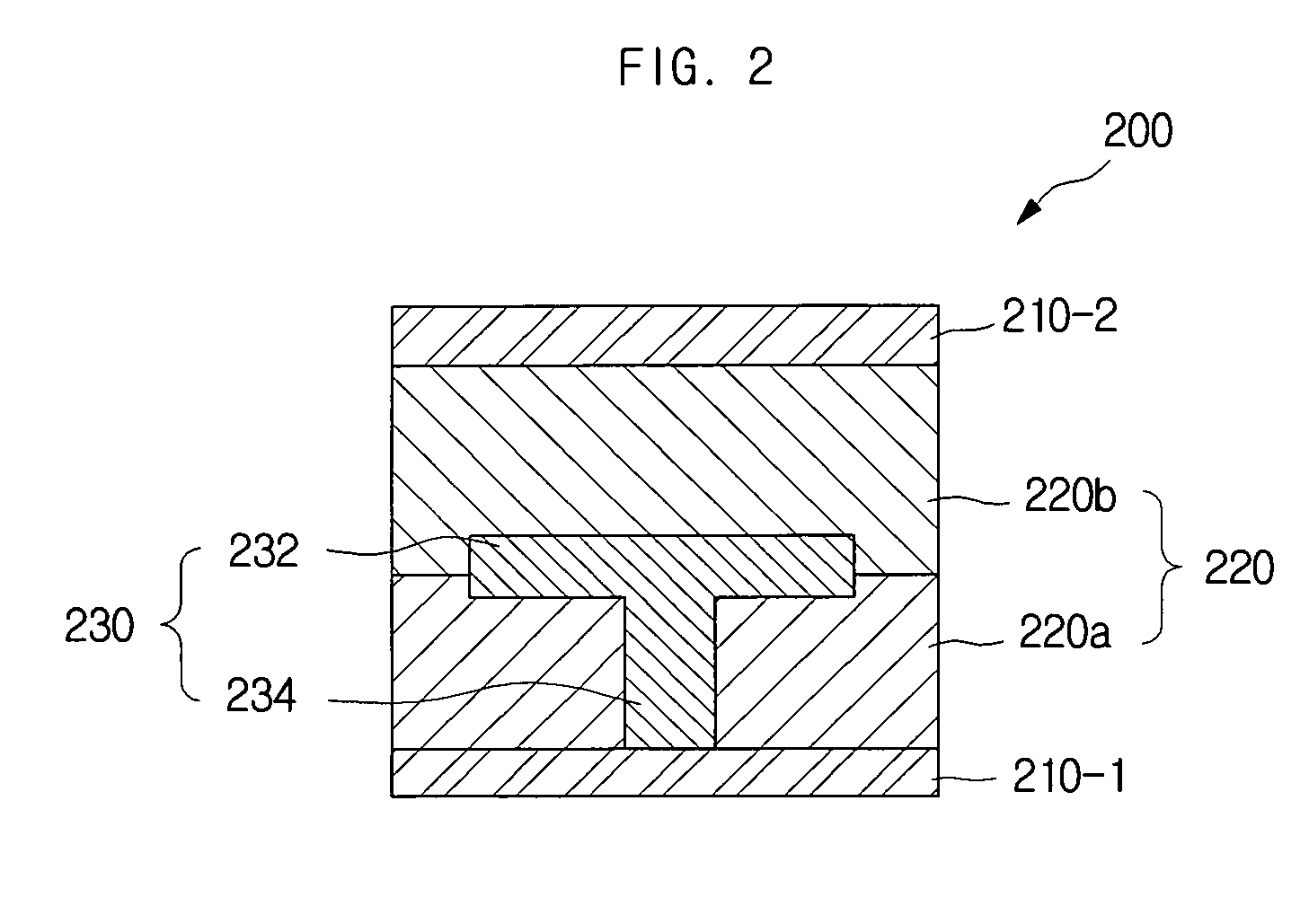
[0046]Since there can be a variety of permutations and embodiments of the present invention, certain embodiments will be illustrated and described with reference to the accompanying drawings. This, however, is by no means to restrict the present invention to certain embodiments, and shall be construed as including all permutations, equivalents and substitutes covered by the spirit and scope of the present invention. Throughout the drawings, similar elements are given similar reference numerals. Throughout the description of the present invention, when describing a certain technology is determined to evade the point of the present invention, the pertinent detailed description will be omitted.

[0047]Terms such as “first” and “second” can be used in describing various elements, but the above elements shall not be restricted to the above terms. The above terms are used only to distinguish one element from the other. For instance, the first element can be named the second element, and vic...


PUM


Abstract

An electromagnetic bandgap structure and a printed circuit board that can solve a mixed signal problem between an analog circuit and a digital circuit are disclosed. In accordance with an embodiment of the present invention, the electromagnetic bandgap structure can include a metal layer; and a plurality of mushroom type structures including a metal plate and a via. Here, the plurality of mushroom type structures can be formed on the metal layer in a stacked structure. With the present invention, the small sized electromagnetic bandgap structure can have a lower bandgap frequency.

Description

CROSS-REFERENCE TO RELATED PATENT APPLICATIONS[0001]This application claims the benefit of Korean Patent Application No. 10-2007-0041991, filed on Apr. 30, 2007, in the Korean Intellectual Property Office, the disclosure of which is incorporated herein in its entirety by reference.BACKGROUND OF THE INVENTION[0002]1. Field of the Invention[0003]The present invention relates to a printed circuit board, more specifically to a printed circuit board that can solve a mixed signal problem between an analog circuit and a digital circuit.[0004]2. Background Art[0005]Various apparatuses such as mobile communication terminals, personal digital assistants (PDA), laptop computers and digital multimedia broadcasting (DMB) devices have been launched in order to meet today's trend that mobility is considered as one of the most important issues.[0006]Such apparatuses include a printed circuit board, which is configured to compound analog circuits (e.g. radio frequency (RF) circuits) and digital circ...

Claims


Application Information

Patent Timeline
30 Oct 2008
Publication
US20080266018A1
IPC
H01P1/20
CPC
H01P1/2005; H05K1/0236; H05K2201/09309; H05K2201/09663; H01Q15/008; H01L2224/16225; H05K1/02
Inventors
HAN, MI-JA; KIM, HAN