Film Formation Method and Method for Manufacturing Light-Emitting Device

a technology of film formation and manufacturing method, which is applied in the direction of electroluminescent light sources, vacuum evaporation coatings, coatings, etc., can solve the problems of reducing manufacturing efficiency, reducing the time required for evacuation of film formation chambers, and reducing so as to reduce the distance between the evaporation source and the substrate on which the film is formed, the interval of maintenance can be extended, and the utilization efficiency of materials can be drastically improved

Inactive Publication Date: 2008-10-30
SEMICON ENERGY LAB CO LTD
View PDF3 Cites 29 Cited by
  • Summary
  • Abstract
  • Description
  • Claims
  • Application Information

AI Technical Summary

Benefits of technology

[0010]It is an object of the present invention to provide a film formation method excellent in throughput, in which a film which is uniform in film thickness and film quality is formed while the manufacturing cost is suppressed by improvement of utilization efficiency of a material, in forming a film. In particular, it is another object of the present invention to obtain uniformity of film formation in which variation in film thickness is in the range of less than 3%.

Problems solved by technology

Further, since a film formation chamber is enlarged, there is a problem in that time required for evacuation of a film formation chamber is increased.
In such maintenance, suspension of part of a manufacturing line is necessary, which results in reduction of manufacturing efficiency.
Thus, there are loss of time taken until the evaporation speed is stabilized and loss of the evaporation material, which results in reduction of manufacturing efficiency.

Method used


Image

  • Film Formation Method and Method for Manufacturing Light-Emitting Device
  • Film Formation Method and Method for Manufacturing Light-Emitting Device
  • Film Formation Method and Method for Manufacturing Light-Emitting Device

Examples


embodiment mode 1

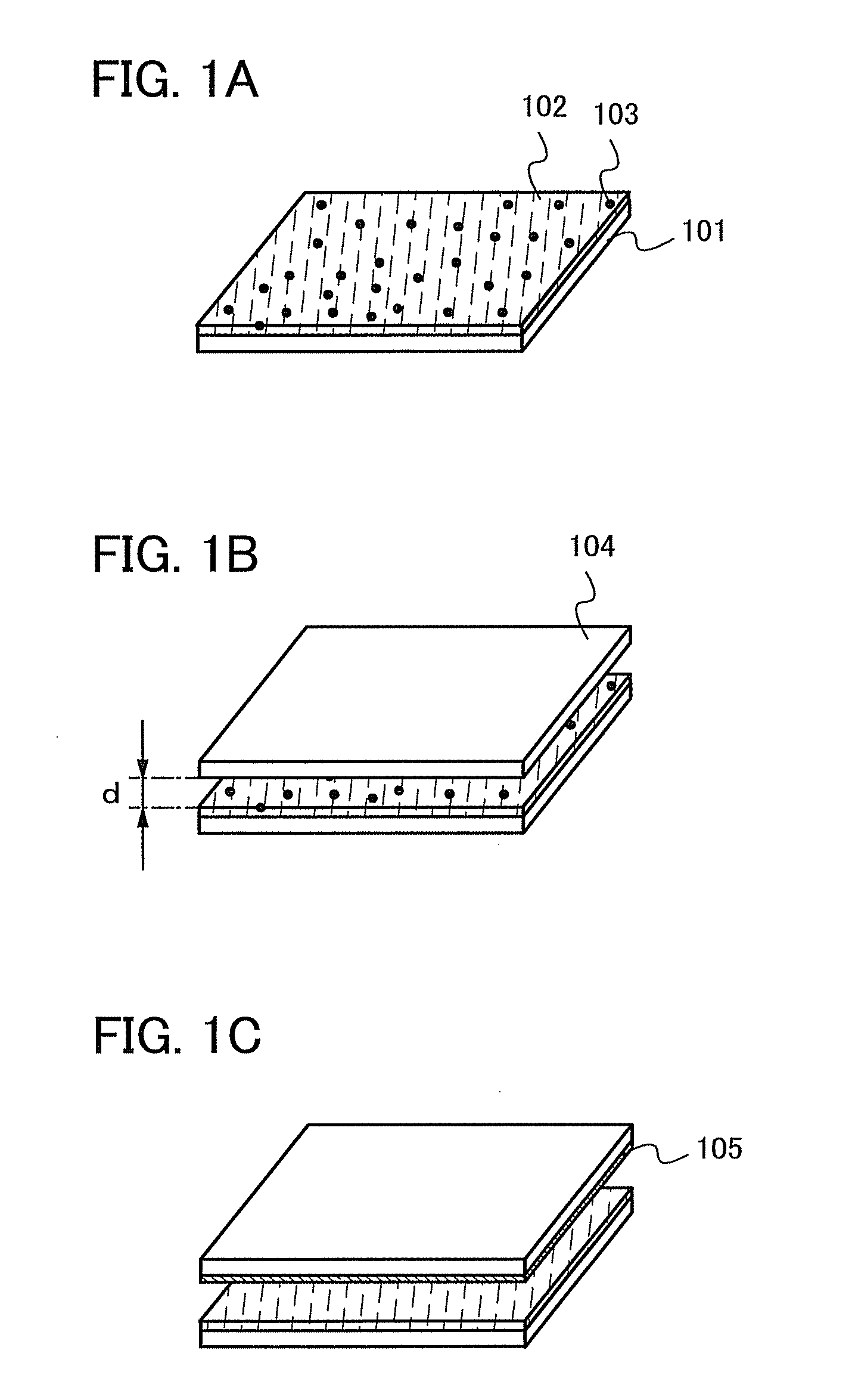
[0066]One mode of a film formation method of the present invention is described with reference to the drawings. FIGS. 1A to 1C are perspective views showing a concept of a film formation method of this embodiment mode.

[0067]First, a first material layer 102 including an evaporation material 103 is formed over a main surface of a first substrate 101 (see FIG. 1A). Here, the first substrate 101 is an evaporation source substrate, and the first material layer 102 is a layer including a mixture of the evaporation material 103 and a binder material. The binder material is a substance of higher molecular weight than the evaporation material 103.

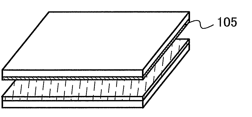
[0068]Next, a second substrate 104 is placed so as to face the first substrate 101 (see FIG. 1B). Here, the second substrate 104 is a substrate on which a film is formed. The second substrate 104 is placed to face the first material layer 102 formed over the first substrate 101. A surface of the first material layer 102 and a surface of the second ...

embodiment mode 2

[0110]This embodiment mode describes an example of a mode of the present invention, which is different from Embodiment Mode 1, with reference to the drawings. In specific, the case is described where a mixture layer is selectively formed over an evaporation source substrate.

[0111]FIGS. 5A to 5C show an example of the case where a mixture layer is selectively formed. Here, a first material layer 202 which is a mixture layer is formed over a first substrate 201 which is an evaporation source substrate by an ink-jet method. First, a mixture layer of an evaporation material 203 and a material of higher molecular weight than the evaporation material 203 is discharged from a head 200, whereby the first material layer 202 is selectively formed over a main surface of the first substrate 201 (see FIG. 5A). Here, the first substrate 201 serves as an evaporation source substrate.

[0112]Next, a second substrate 204 is placed so as to face the first substrate 201 (see FIG. 5B). Here, the second s...

embodiment mode 3

[0117]This embodiment mode describes an example of a mode of the present invention, which is different from Embodiment Mode 1, with reference to the drawings. In specific, the case is described where a thermally conductive layer is selectively formed over an evaporation source substrate and a binder material layer is formed over the evaporation source substrate and the thermally conductive layer.

[0118]FIGS. 6A to 6D show an example of the case where a thermally conductive layer is selectively formed. Here, a thermally conductive layer 302 is formed over the first substrate 301 by an ink-jet method. First, a material which forms the thermally conductive layer 302 is discharged from a head 300 to selectively form the thermally conductive layer 302 over a main surface of the first substrate 301 (see FIG. 6A). Here, the first substrate 301 serves as an evaporation source substrate.

[0119]The thermally conductive layer is not particularly limited as long as it is formed from a material wi...


PUM

PropertyMeasurementUnit
sublimation temperatureaaaaaaaaaa
sizeaaaaaaaaaa
sizeaaaaaaaaaa

Abstract

A binder material layer including an evaporation material is formed over a main surface of an evaporation source substrate, a substrate on which a film is formed is placed so that the binder material layer and a main surface thereof face each other, and heat treatment is performed on a rear surface of the evaporation source substrate so that the evaporation material in the binder material layer is heated to be subjected to sublimation or the like, whereby a layer of the evaporation material is formed on the substrate on which a film is formed. When a low molecular material is used for the evaporation material and a high molecular material is used for the binder material, the viscosity can be easily adjusted, and thus, film formation is possible with higher throughput than conventional film formation.

Description

BACKGROUND OF THE INVENTION[0001]1. Field of the Invention[0002]The present invention relates to a film formation method by which a film is formed over a substrate. Further, the present invention relates to a method for manufacturing a light-emitting device in which a layer including an organic compound which is manufactured by the film formation method is used as a light-emitting layer.[0003]2. Description of the Related Art[0004]In recent years, a technique relating to a flat panel display has been remarkably progressed. As a typical flat panel display, a liquid crystal display device and a light-emitting device can be given.[0005]A liquid crystal display device operates by control of transmittance of light, which is emitted from a backlight, at each pixel by liquid crystal elements arranged in matrix. A light-emitting device operates by control of a lighting state or a non-lighting state of self-light-emitting elements arranged in matrix at each pixel. As compared to a liquid cry...

Claims


Application Information

Patent Timeline
Patent Type & Authority Applications(United States)
IPC IPC(8): B05D5/12C23C14/34C23C14/12C23C14/24H01L51/50H05B33/10
CPCC23C14/12H01L51/001H01L51/0038H01L51/0042H01L51/0059H01L51/006C23C16/4485B05D2401/30C23C14/00C23C14/042C23C14/24C23C14/26H05B33/10H10K71/164H10K85/146H10K85/114H10K85/633H10K85/631H01L21/205H01L21/20H05B33/14H01L21/324
Inventor IKEDA, HISAOIBE, TAKAHIROAOYAMA, TOMOYA
Owner SEMICON ENERGY LAB CO LTD
Why Eureka
Try Eureka