Process for forming cobalt and cobalt silicide materials in copper contact applications

a technology of cobalt silicide and cobalt silicide, which is applied in the direction of coatings, chemical vapor deposition coatings, semiconductor devices, etc., can solve the problems of reducing the reliability of the overall circuit, difficult to integrate cobalt silicide processes into conventional manufacturing equipment, and cobalt agglomeration

Inactive Publication Date: 2008-10-30
APPLIED MATERIALS INC
View PDF104 Cites 378 Cited by
  • Summary
  • Abstract
  • Description
  • Claims
  • Application Information

AI Technical Summary

Benefits of technology

[0029]In some examples, the reagent may contain a reducing agent, such as hydrogen, silane, disilane, diborane, ammonia, phosphine, derivatives thereof, plasmas thereof, or combinations thereof. The substrate may be exposed to a plasma during the treatment process. In other examples the apertures may be filled with a copper bulk layer by depositing copper therein and over the copper seed layer during a bottom-up deposition process, such as a PVD process, an ECP process, or an electroless deposition process.
[0030]In another embodiment, a method for forming a cobalt silicide containing material on a substrate is provided which includes treating the substrate with at least one preclean process to expose a silicon-containing surface, depositing a cobalt silicide material over the silicon-containing surface, depositing a metallic cobalt material over the cobalt silicide material, exposing the metallic cobalt material to a reducing agent during a pre-treatment process, and depositing a copper seed layer over the metallic cobalt material during a CVD process or an ALD process.

Problems solved by technology

However, it has been difficult to integrate cobalt silicide processes into conventional manufacturing equipment.
Transfer between chambers may expose the substrate to contamination and potential oxidation of silicon or cobalt deposited on the substrate surface.
Oxide formation on the surface of the substrate can result in increasing the resistance of silicide layers as well as reducing the reliability of the overall circuit.
For example, oxidation of the deposited cobalt material may result in cobalt agglomeration and irregular growth of the cobalt silicide layer.
The agglomeration and irregular growth of the cobalt silicide layer may result in device malformation, such as source and drain electrodes having different thicknesses and surface areas.
Additionally, excess cobalt silicide growth on substrate surface may form conductive paths between devices, which may result in short circuits and device failure.
However, the addition of titanium and titanium nitride deposition and removal processes increases the number of processing steps required for silicide formation, thereby reducing process efficiency, increasing processing complexity, and reducing substrate throughput.
However, deposition of titanium over silicon surfaces presents the problem of titanium silicide formation.
Titanium silicide has been observed to agglomerate, which detrimentally affects subsequently deposited materials.
Also, titanium silicide exhibits a radical increase in sheet resistance as feature sizes decrease below 0.17 μm, which detrimentally affects the conductance of the feature being formed.
Further, titanium silicide has an insufficient thermal stability during processing of the substrate at temperatures of about 400° C. or higher, which can result in interlayer diffusion and detrimentally affect device performance.
This results in difficult integration of PVD and CVD processes in the same system.
The increase in the number of systems results in increased production costs, increased production times, and exposes the processed substrate to contamination when transferred between systems.

Method used


Image

  • Process for forming cobalt and cobalt silicide materials in copper contact applications
  • Process for forming cobalt and cobalt silicide materials in copper contact applications
  • Process for forming cobalt and cobalt silicide materials in copper contact applications

Examples


example 1

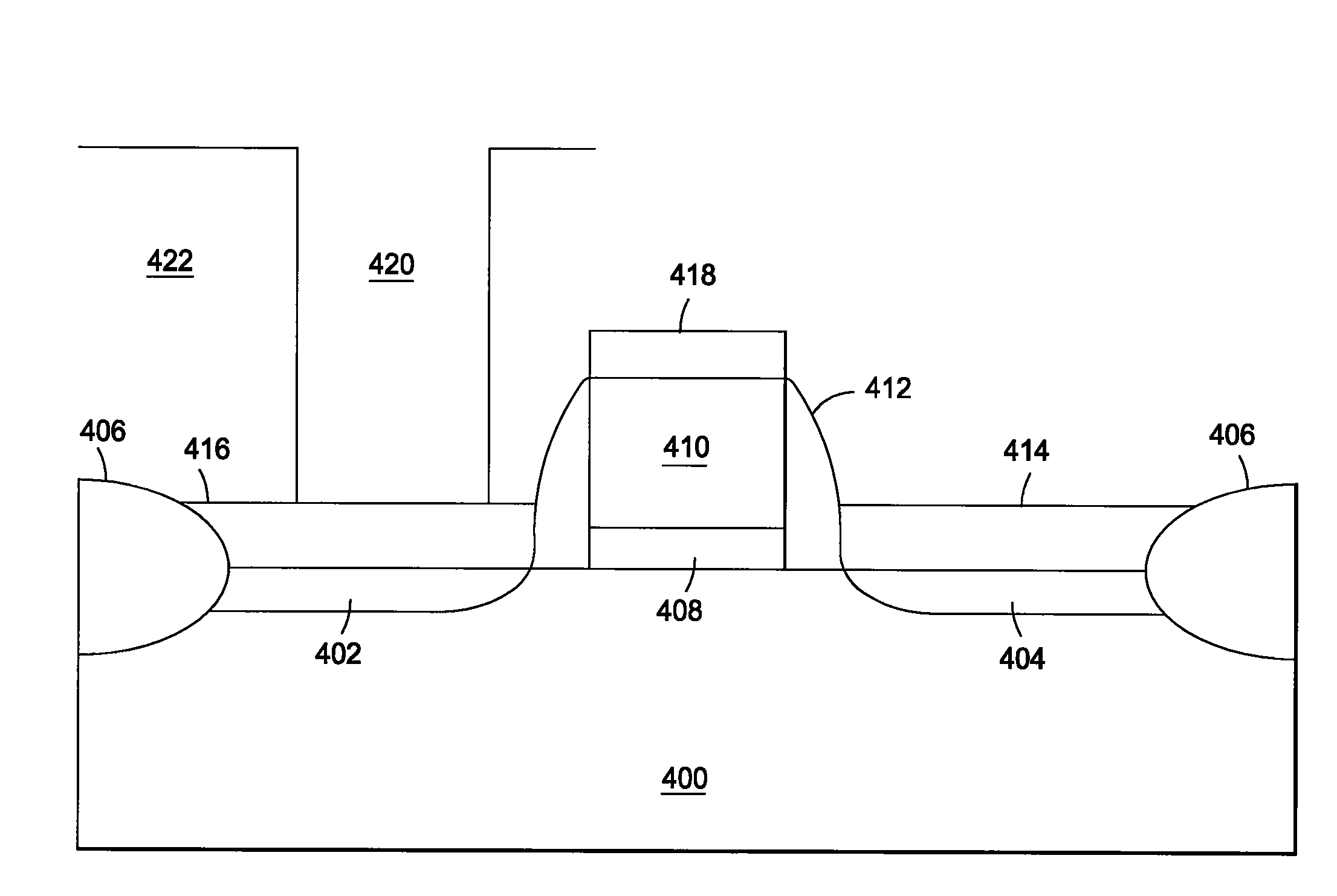
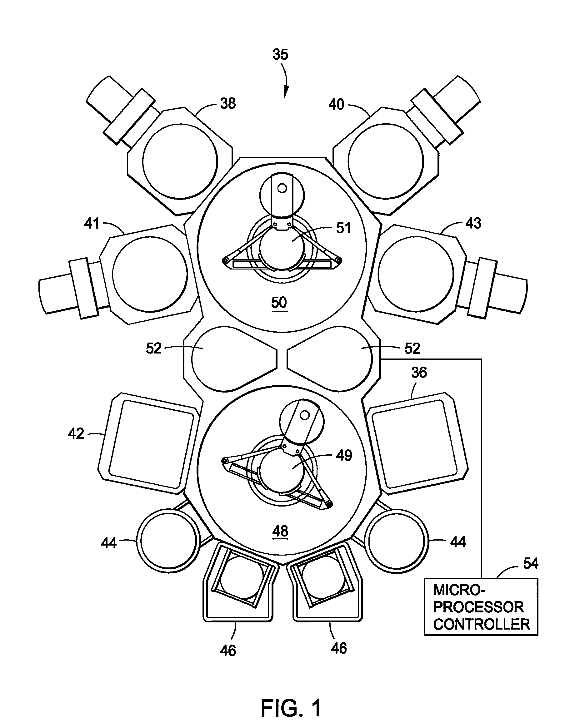
[0324]A substrate is treated with at least one preclean process to expose a silicon-containing surface, a cobalt silicide material is deposited over the silicon-containing surface, a metallic cobalt material is deposited over the cobalt silicide material, an optional treatment process may be used to remove cobalt oxides or other surface contaminants, a tungsten material is deposited over the metallic cobalt material, and the tungsten material is exposed to a CMP process. The metallic cobalt material and the cobalt silicide material may be deposited in a first processing chamber, and the optional treatment and the deposition of the tungsten material may be performed in a second processing chamber.

example 2

[0325]A substrate is treated with at least one preclean process to expose a silicon-containing surface, a cobalt silicide material is deposited over the silicon-containing surface, an optional treatment process may be used to remove cobalt oxides or other surface contaminants, a tungsten material (e.g., metallic tungsten) is deposited over the cobalt silicide material, and the tungsten material is exposed to a CMP process. The cobalt silicide material may be deposited in a first processing chamber and the optional treatment and the deposition of the tungsten material may be performed in a second processing chamber.

example 3

[0326]A substrate is treated with at least one preclean process to expose a silicon-containing surface, a cobalt silicide material is deposited over the silicon-containing surface, a metallic cobalt material is deposited over the cobalt silicide material, the substrate is exposed to an annealing process, an optional treatment process may be used to remove cobalt oxides or other surface contaminants, a tungsten material is deposited over the metallic cobalt material, and the tungsten material is exposed to a CMP process. The deposition of the metallic cobalt material and the cobalt silicide material and the annealing process may be performed in a first processing chamber, and the optional treatment and the deposition of the tungsten material may be performed in a second processing chamber.


PUM

PropertyMeasurementUnit
sizeaaaaaaaaaa
temperaturesaaaaaaaaaa
temperatureaaaaaaaaaa

Abstract

Embodiments of the invention described herein generally provide methods for forming cobalt silicide layers and metallic cobalt layers by using various deposition processes and annealing processes. In one embodiment, a method for forming a cobalt silicide material on a substrate is provided which includes treating the substrate with at least one preclean process to expose a silicon-containing surface, depositing a cobalt silicide material over the silicon-containing surface, and depositing a copper material over the cobalt silicide material. In another embodiment, a metallic cobalt material may be deposited over the cobalt silicide material prior to depositing the copper material. In one example, the copper material may be formed by depositing a copper seed layer and a copper bulk layer on the substrate. The copper seed layer may be deposited by a PVD process and the copper bulk layer may be deposited by an ECP process or an electroless deposition process.

Description

CROSS-REFERENCE TO RELATED APPLICATIONS[0001]This application is a continuation-in-part of U.S. Ser. No. 11 / 733,929 (APPM / 005547.P2), filed Apr. 11, 2007, which claims benefit of U.S. Ser. No. 60 / 791,366 (APPM / 010948L), filed Apr. 11, 2006, and U.S. Ser. No. 60 / 863,939 (APPM / 010948L.02), filed Nov. 1, 2006, and which is also a continuation-in-part of U.S. Ser. No. 11 / 456,073 (APPM / 005547.C2), filed Jul. 6, 2006, which is a continuation of U.S. Ser. No. 10 / 845,970 (APPM / 005547.C1), filed May 14, 2004, and now abandoned, which is a continuation of U.S. Ser. No. 10 / 044,412 (APPM / 005547.P1), filed Jan. 9, 2002, and issued as U.S. Pat. No. 6,740,585, which is a continuation-in part of U.S. Ser. No. 09 / 916,234 (APPM / 005547), filed Jul. 25, 2001, and now abandoned, which are all herein incorporated by reference in their entirety.BACKGROUND OF THE INVENTION[0002]1. Field of the Invention[0003]Embodiments of the invention relate to the fabrication of semiconductor and other electronic device...

Claims


Application Information

Patent Timeline
Patent Type & Authority Applications(United States)
IPC IPC(8): H01L21/44
CPCC23C16/0227C23C16/08C23C16/18C23C16/42C23C16/4554C23C16/4586C23C16/56H01L21/28518H01L21/2855H01L21/28556H01L21/28562H01L21/76843H01L21/76846H01L21/76855H01L21/76877H01L29/665H01L29/78
Inventor YU, SANG-HOMORAES, KEVIN TIGANGULI, SESHADRICHUNG, HUAPHAN, SEE-ENGKHANDELWAL, AMITWU, KAI
Owner APPLIED MATERIALS INC
Why Eureka
Try Eureka