Image sensor and method of manufacturing the same

a technology of image sensor and manufacturing method, applied in the direction of electrical apparatus, semiconductor devices, radio frequency controlled devices, etc., can solve the problems of noise and crosstalk, bridge and merge of microlenses, gaps between microlenses, etc., and achieve the effect of minimizing gaps

Active Publication Date: 2008-11-06
DONGBU HITEK CO LTD
View PDF2 Cites 160 Cited by
  • Summary
  • Abstract
  • Description
  • Claims
  • Application Information

AI Technical Summary

Benefits of technology

[0010]Embodiments of the present invention provide an image sensor and a method of manufacturing the image se

Problems solved by technology

Here, light passing through the gaps may be detected by a non-corresponding photodiode disposed on the pixel array substrate, which produces noise and crosstalk.
The gaps form between microlenses when wide areas between the microlenses in

Method used


Image

  • Image sensor and method of manufacturing the same
  • Image sensor and method of manufacturing the same
  • Image sensor and method of manufacturing the same

Examples


Embodiment Construction

[0015]Reference will now be made in detail to embodiments of the present disclosure, examples of which are illustrated in the accompanying drawings.

[0016]When the terms “on” or “over” are used herein, when referring to layers, regions, patterns, or structures, it is understood that the layer, region, pattern or structure can be directly on another layer or structure, or intervening layers, regions, patterns, or structures may also be present. When the terms “under” or “below” are used herein, when referring to layers, regions, patterns, or structures, it is understood that the layer, region, pattern or structure can be directly under the other layer or structure, or intervening layers, regions, patterns, or structures may also be present.

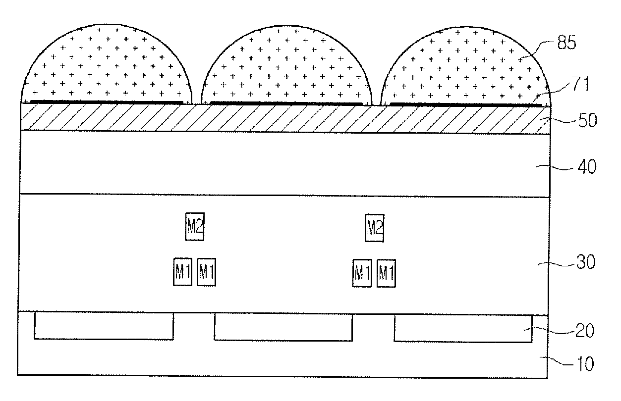
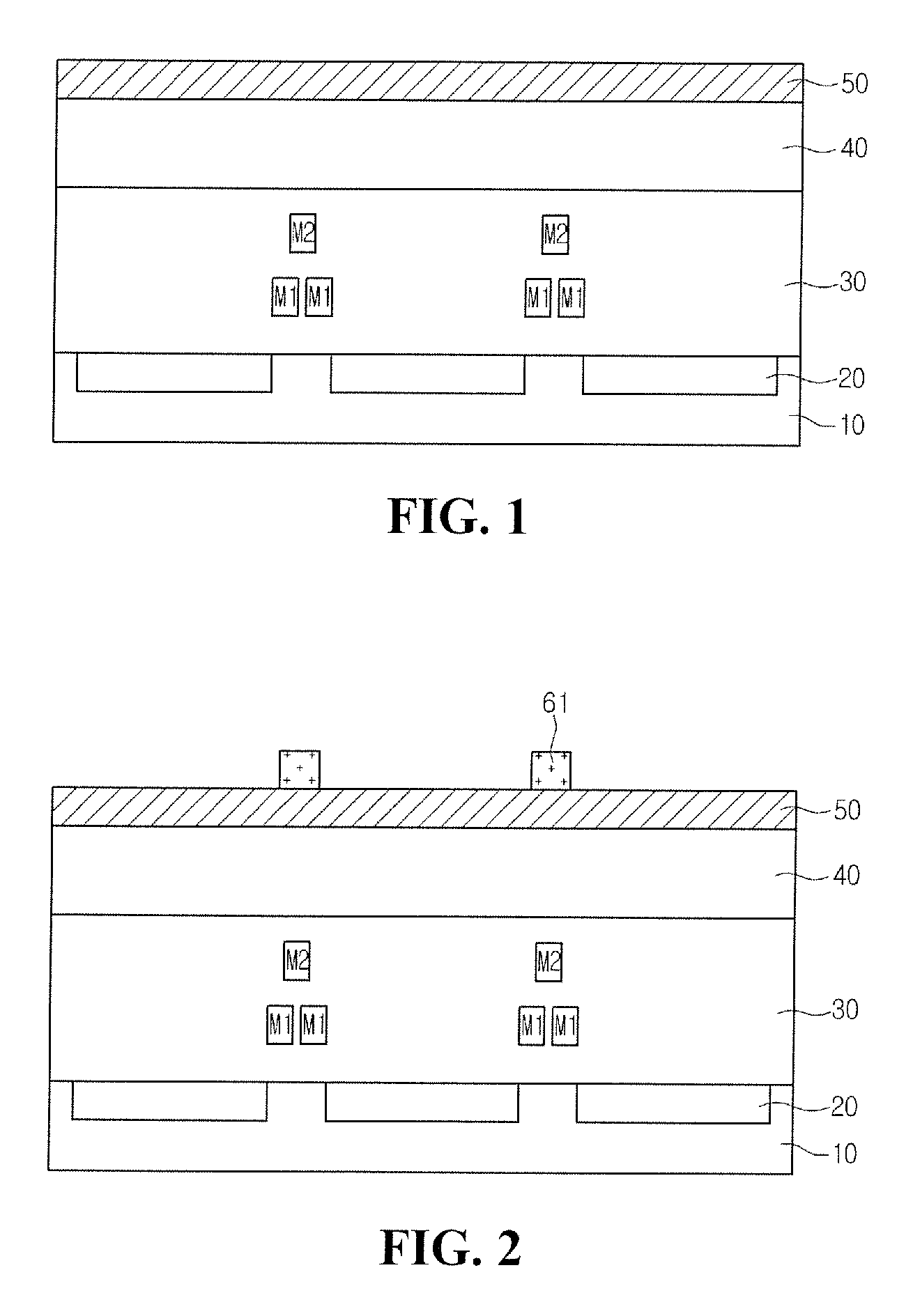
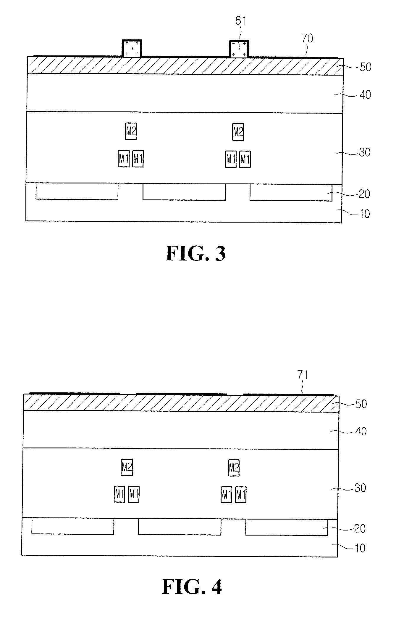
[0017]FIG. 6 is a cross-sectional view illustrating an image sensor according to an embodiment.

[0018]Referring to FIG. 6, an image sensor can include a semiconductor substrate 10 including unit pixels, a metal interconnection layer 30 on the semicon...


PUM


Abstract

Provided is an image sensor and method of manufacturing the same. The image sensor can include a semiconductor substrate, a metal interconnection layer, an inorganic layer, lens seed patterns, and microlenses. The semiconductor substrate can include unit pixels. The metal interconnection layer can be disposed on the semiconductor substrate to provide signal and poser connections to the unit pixels. The inorganic layer can be disposed on the metal interconnection layer. The lens seed patterns are selectively disposed on the inorganic layer and are formed of an organic material. The microlenses are formed on the lens seed patterns.

Description

CROSS-REFERENCE TO RELATED APPLICATIONS[0001]The present application claims the benefit under 35 U.S.C. §119 of Korean Patent Application No. 10-2007-0042911, filed May 3, 2007, which is hereby incorporated by reference in its entirety.BACKGROUND[0002]In general, an image sensor is a semiconductor device that converts an optical image into an electrical signal. The image sensor is typically classified as a charge coupled device (CCD) image sensor or a complementary metal oxide semiconductor (CMOS) image sensor (CIS).[0003]A unit pixel of such a CIS includes a photodiode and a metal oxide semiconductor (MOS) transistor. In operation, the CIS sequentially detects an electrical signal of the unit pixel in a switching manner to generate an image.[0004]To improve optical sensitivity of the CIS, microlenses are used to condense light towards the photodiodes. Color filters are also included in certain CIS to produce a color image.[0005]The color filters and the microlenses are formed on a ...

Claims


Application Information

Patent Timeline
IPC IPC(8): H01L31/00H01L21/00H01L31/113
CPCH01L27/14627H01L27/14685H01L27/146
Inventor YUN, YOUNG JE
Owner DONGBU HITEK CO LTD
Why Eureka
Try Eureka