Chip package structure

a chip and package technology, applied in the field of packaging, can solve the problems of increasing the defect rate of products and inner stress, and achieve the effect of reducing inner stress and high yield

Inactive Publication Date: 2008-11-06
ADVANCED SEMICON ENG INC
View PDF5 Cites 47 Cited by
  • Summary
  • Abstract
  • Description
  • Claims
  • Application Information

AI Technical Summary

Benefits of technology

[0006]The present invention is directed to a chip package structure, which includes a carrier, an interposer, a plurality of first electrically conductive elements, a first sealant, a chip, and a second sealant. A plurality of connection pads is disposed on an upper surface of the carrier, and a plurality of ball pads is disposed on a lower surface of the carrier. The interposer is disposed on the upper surface of the carrier, and has a first surface, a second surface, and a plurality of vias. The vias electrically conduct a plurality of first contacts of the first surface and a plurality of second contacts of the second surface. The first electrically conductive elements are disposed between the carrier and the interposer, and electrically connect the interposer and the carrier. The first sealant seals the first electrically c

Problems solved by technology

However, in the process of packaging, since the carrier, the chip, and the interposer have different coefficients of thermal expansion, but use the same sealant, the carrier, the chip, and the interposer

Method used


Image

  • Chip package structure
  • Chip package structure

Examples


Embodiment Construction

[0011]Reference will now be made in detail to the present preferred embodiments of the invention, examples of which are illustrated in the accompanying drawings. Wherever possible, the same reference numbers are used in the drawings and the description to refer to the same or like parts.

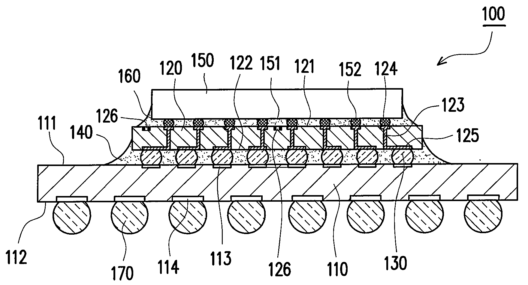
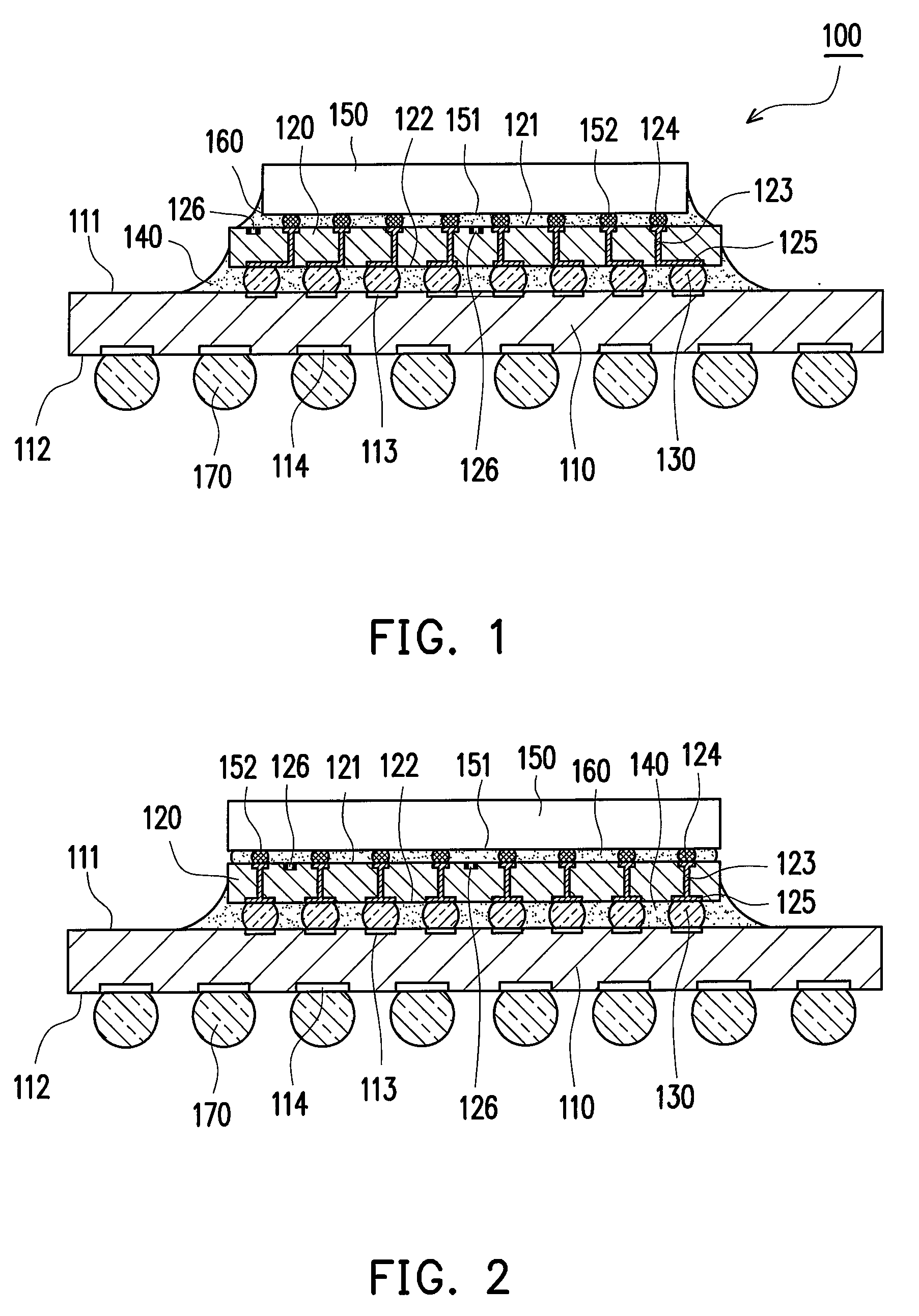
[0012]Referring to FIG. 1, in an embodiment of the present invention, a chip package structure 100 including a carrier 110, an interposer 120, a plurality of first electrically conductive elements 130, a first sealant 140, a chip 150, and a second sealant 160 is provided. The carrier 110 has an upper surface 111 and a lower surface 112. The carrier 110 may be an organic substrate or a lead frame. In this embodiment, the carrier 110 is an organic substrate. A plurality of connection pads 113 is disposed on the upper surface 111, and a plurality of ball pads 114 is disposed on the lower surface 112. The interposer 120 is disposed on the upper surface 111 of the carrier 110, and the material of the inte...


PUM


Abstract

A chip package structure includes a carrier, an interposer, a plurality of electrically conductive elements, a first sealant, a chip, and a second sealant. The interposer is disposed on the carrier. The electrically conductive elements electrically connect the interposer and the carrier. The first sealant seals the electrically conductive elements. A plurality of bumps of the chip is connected to the interposer. The second sealant seals the bumps. A first glass transition temperature of the first sealant is higher than a second glass transition temperature of the second sealant. Since glass transition temperatures of the first sealant and the second sealant are different, and the first glass transition temperature of the first sealant is higher than the second glass transition temperature of the second sealant, the inner stress will be lowered and the yield is promoted.

Description

CROSS-REFERENCE TO RELATED APPLICATION[0001]This application claims the priority benefit of Taiwan application serial no. 96116028, filed on May 4, 2007. The entirety of the above-mentioned patent application is hereby incorporated by reference herein and made a part of this specification.BACKGROUND OF THE INVENTION[0002]1. Field of the Invention[0003]The present invention generally relates to a package, in particular, to a chip package structure.[0004]2. Description of Related Art[0005]A conventional package mainly includes a carrier, a chip, an interposer, and a sealant. The chip may be electrically connected to the interposer through a plurality of bumps of the chip. The interposer may be electrically connected to the carrier through a plurality of electrically conductive elements. In order to protect the bumps of the chip and the electrically conductive elements, the sealant must seal the bumps and the electrically conductive elements. However, in the process of packaging, since...

Claims


Application Information

Patent Timeline
IPC IPC(8): H01L23/488
CPCH01L21/563H01L23/147H01L23/49816H01L23/49827H01L23/49833H01L24/16H01L24/32H01L2224/16H01L2224/73203H01L2924/15311H05K1/141H05K2201/10378H05K2201/10674H05K2201/10977H01L2924/00014H01L2924/00011H01L2224/0401
Inventor WANG, WEI-CHUNGWANG, MENG-JENWANG, TONG-HONG
Owner ADVANCED SEMICON ENG INC
Why Eureka
Try Eureka