
Solid state imaging device, semiconductor wafer, optical device module, method of solid state imaging device fabrication, and method of optical device module fabrication

a solid-state imaging and semiconductor technology, applied in the direction of machines/engines, radio-controlled devices, television systems, etc., can solve the problems of reducing the size of the device, and affecting the operation of the device. , to achieve the effect of reducing the size of the solid-state imaging device, high environmental durability, and high reliability

Inactive Publication Date: 2008-11-13
SHARP KK
View PDF16 Cites 14 Cited by
  • Summary
  • Abstract
  • Description
  • Claims
  • Application Information

AI Technical Summary

Benefits of technology

[0012]The invention has been devised with considering such problems. An object of the invention is to provide a solid state imaging device in which a light-transparent cover having planar dimensions smaller than those of a solid state image pickup device is adhered opposite to the effective pixel region in one surface of the solid state image pickup device, so as to protect the effective pixel region such as to prevent external influences (such as moisture and dust) from affecting the surface of the effective pixel region, and in which at the same time, the size of the solid state imaging device is reduced so that a solid state imaging device of a chip size having high reliability and high environmental durability is realized.
[0013]Another object of the invention is to provide a semiconductor wafer on which a plurality of solid state image pickup devices are formed, in which a light-transparent plate or a light-transparent cover for protecting the surface of the effective pixel region of solid state image pickup device is formed before the dividing of the solid state image pickup devices into individual pieces, so as to permit easy storage and carriage and avoid the attachment of dust or the occurrence of damage to the surface of the effective pixel region after the process of dividing the solid state image pickup devices into individual pieces, so that the fraction defective is reduced in the process of assembling the solid state image pickup device especially after the dividing into individual pieces.
[0014]Another object of the invention is to provide an optical device module such as a camera module permitting easy size reduction and having good portability by means of incorporating a solid state imaging device according to the invention.

Problems solved by technology

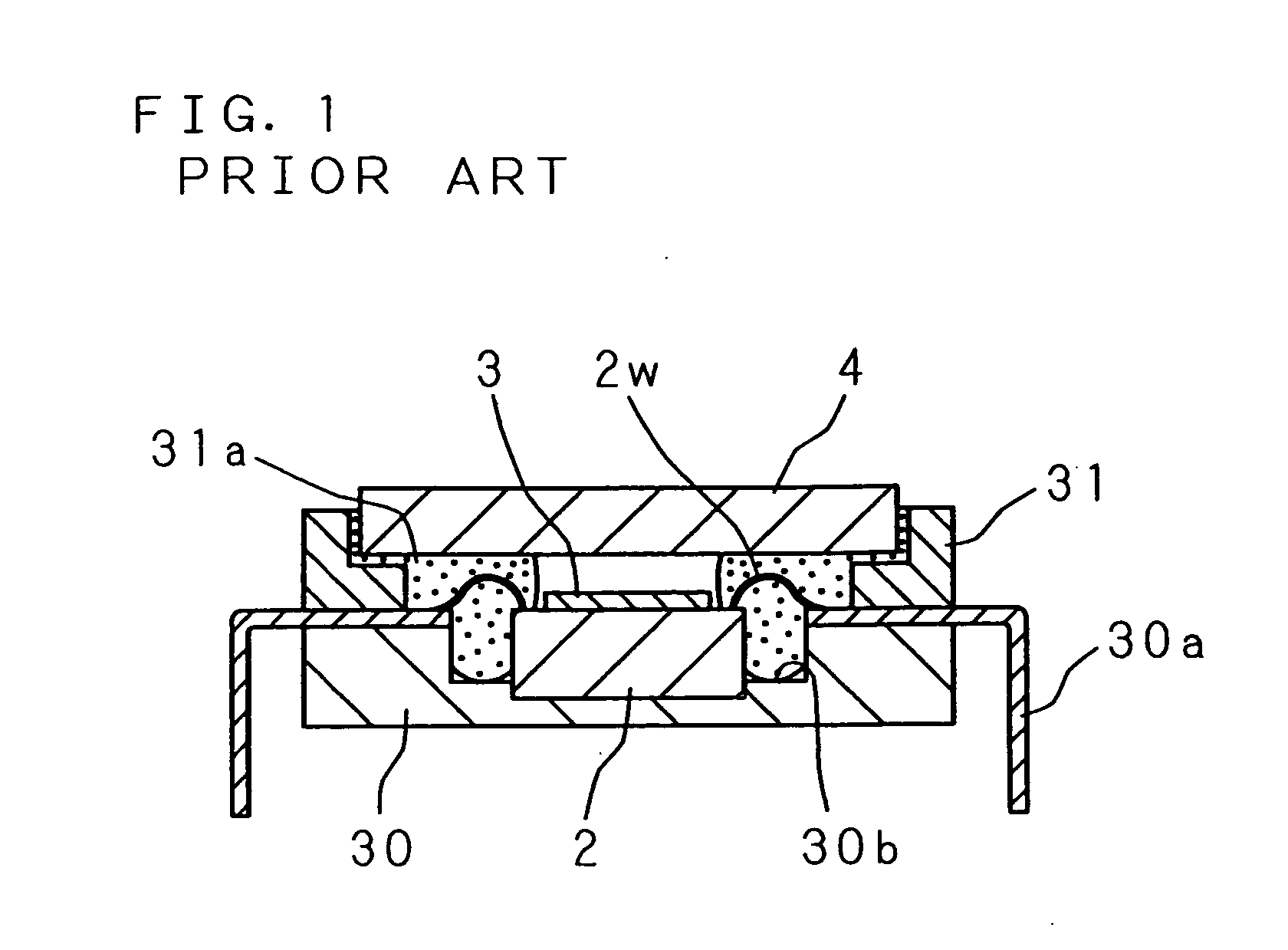
That is, the above-mentioned structure that the light-transparent cover 4 covers not only the effective pixel region 3 alone but also the entirety, or even also the outer region, of the solid state image pickup device 2 is disadvantageous in the size reduction.
This causes a possibility of resulting damage to the surface of the effective pixel regions 3 of the solid state image pickup devices 2.
Further, in the process of mounting the solid state image pickup device 2 into the recess 30b of the base 30 using a vacuum chuck handler, there is another possibility of causing damage to the surface of the effective pixel regions 3 of the solid state image pickup devices 2.
Such situation has narrowed the allowable range of fabrication conditions, and hence resulted in a limit in the reduction of the fraction defective in the processes after the dividing of the solid state image pickup device 2 into an individual piece.
This has caused the problem that this largeness restricts the size reduction of the solid state imaging device.
This has caused the problem that the reduction or avoidance of the occurrence of damage to the surface of the effective pixel region of the solid state image pickup device is notably difficult, and that the reduction of the fraction defective is limited.

Method used


Image

  • Solid state imaging device, semiconductor wafer, optical device module, method of solid state imaging device fabrication, and method of optical device module fabrication
  • Solid state imaging device, semiconductor wafer, optical device module, method of solid state imaging device fabrication, and method of optical device module fabrication
  • Solid state imaging device, semiconductor wafer, optical device module, method of solid state imaging device fabrication, and method of optical device module fabrication

Examples


embodiment 1

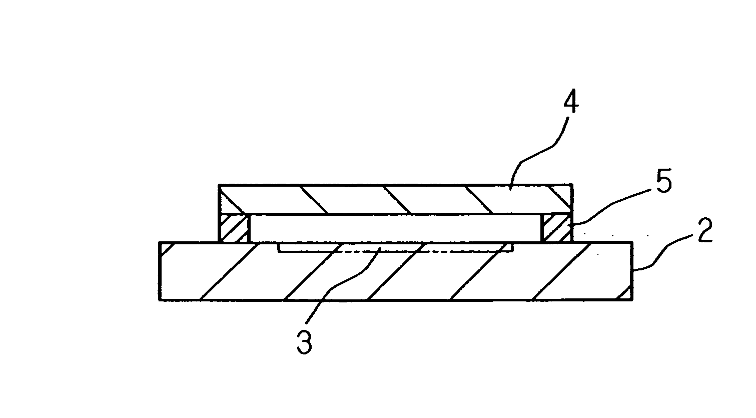
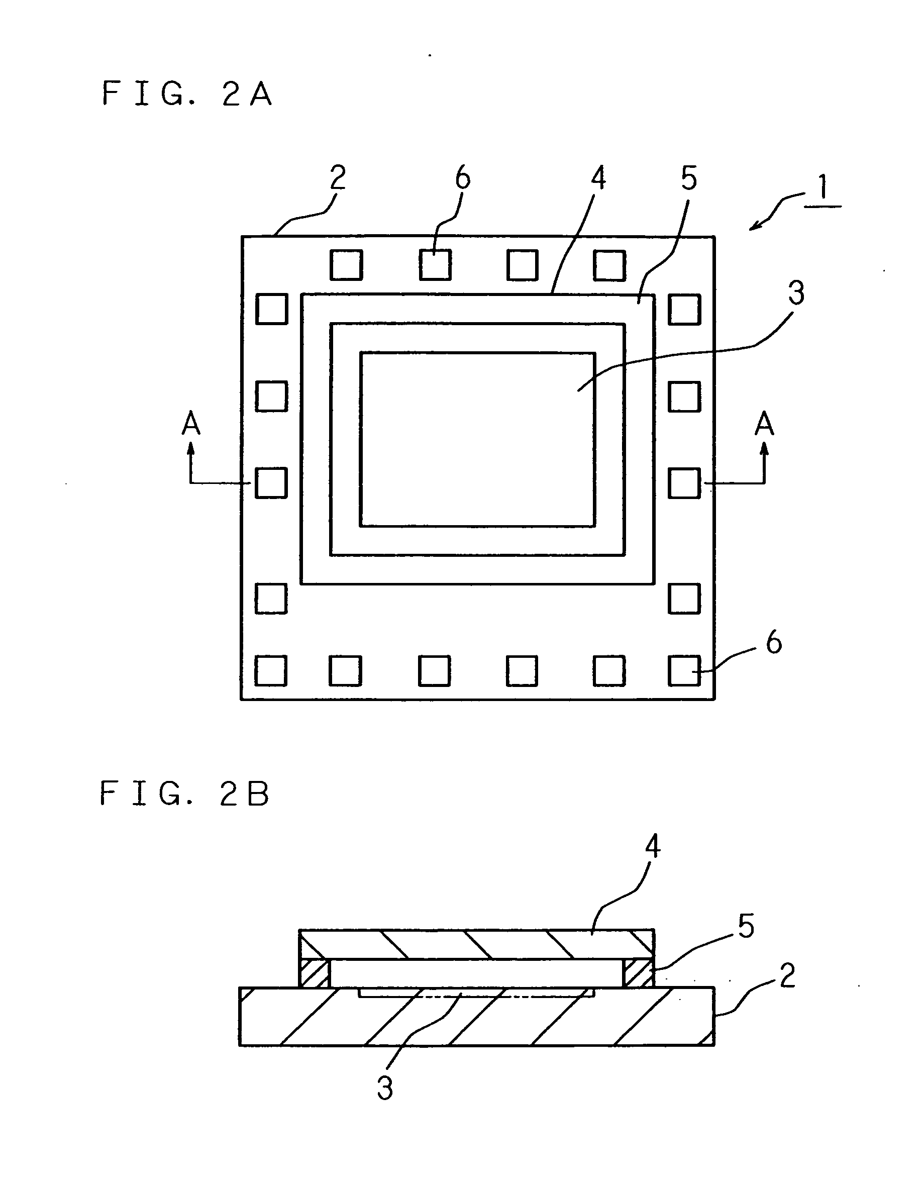
[0088]FIGS. 2A and 2B are diagrams illustrating schematic configuration of a solid state imaging device according to Embodiment 1 of the invention. FIG. 2A is a plan view of the solid state imaging device viewed in a plane (one plane or one surface). FIG. 2B is a cross sectional view along the arrow line A-A in FIG. 2A. Numeral 1 indicates the solid state imaging device comprising: a solid state image pickup device 2 formed in a plan-view shape of a rectangle on a semiconductor substrate; a light-transparent cover 4 arranged opposite to an effective pixel region 3 in order to protect (the surface of) the effective pixel region 3 formed in one surface of the solid state image pickup device 2 against moisture, dust (particles and shavings), and the like in the outside; and an adhering section 5 formed outside the effective pixel region 3 in one surface of the solid state image pickup device 2 so as to adhere the light-transparent cover 4 and the solid state image pickup device 2.

[0089...

embodiment 2

[0093]FIGS. 3A-5B are diagrams illustrating a method of solid state imaging device fabrication according to Embodiment 2 of the invention. More specifically, FIGS. 3A-3E are diagrams illustrating the process of formation of light-transparent covers. FIGS. 4A and 4B are diagrams illustrating the situation of solid state image pickup devices formed on a semiconductor wafer. FIGS. 5A and 5B are diagrams illustrating the situation that the light-transparent covers formed in FIGS. 3A-3E are adhered to one surface (that has the effective pixel regions) of the solid state image pickup devices of FIGS. 4A and 4B.

[0094]FIG. 3A shows a large-area light-transparent plate 10 composed of a glass plate or the like. The light-transparent plate 10 has a large area, and hence comprises a large number of cover corresponding regions 10b having boundaries indicated by dividing lines 10a. The area of the cover corresponding region 10b is adjusted appropriately such as to have the same planar dimensions ...

embodiment 3

[0105]FIGS. 6A-7C are diagrams illustrating a method of solid state imaging device fabrication according to Embodiment 3 of the invention. More specifically, FIGS. 6A and 6B are diagrams illustrating the process of formation of light-transparent covers. FIGS. 7A-7C are diagrams illustrating the process that the light-transparent covers formed in FIGS. 6A and 6B are adhered to one surface (that has the effective pixel regions) of the solid state image pickup devices formed on a semiconductor wafer.

[0106]FIG. 6A shows a large-area light-transparent plate 10 composed of a glass plate or the like. The light-transparent plate 10 has a large area, and hence comprises a large number of cover corresponding regions 10b having boundaries indicated by dividing lines 10a. The area of the cover corresponding region 10b is adjusted appropriately such as to have the same planar dimensions as the light-transparent cover 4 when divided in a later process. FIG. 6B shows the state that the light-trans...


PUM


Abstract

With the reduced size of a solid state imaging device, the invention provides: a solid state imaging device of a chip size and having good environmental durability; a semiconductor wafer used for fabricating a solid state imaging device; an optical device module incorporating a solid state imaging device; a method of solid state imaging device fabrication; and a method of optical device module fabrication. The solid state imaging device comprises: a solid state image pickup device formed on a semiconductor substrate; a light-transparent cover arranged opposite to an effective pixel region, so as to protect (the surface of) the effective pixel region formed in one surface of the solid state image pickup device against external environment; and an adhering section formed outside the effective pixel region in the one surface of the solid state image pickup device, so as to adhere the light-transparent cover and the solid state image pickup device.

Description

[0001]This Nonprovisional application claims priority under 35 U.S.C. § 119(a) on Patent Application No. 2003-29093 filed in Japan on Feb. 6, 2003, and Patent Application No. 2003-53165 filed in Japan on Feb. 28, 2003, the entire contents of which are hereby incorporated by reference.BACKGROUND OF THE INVENTION[0002]The present invention relates to a solid state imaging device used in imaging in a portable phone or the like, a semiconductor wafer used in the fabrication of a solid state imaging device, an optical device module using a solid state imaging device, a method of solid state imaging device fabrication, and a method of optical device module fabrication.DESCRIPTION OF THE RELATED ART[0003]In an area sensor or a linear sensor using a solid state image pickup device such as a CCD, the solid state image pickup device is contained and sealed in a hollow package formed of ceramic or plastic, so that moisture and dust in the outside are prevented from entering the package. Exampl...

Claims


Application Information

Patent Timeline
Patent Type & Authority Applications(United States)
IPC IPC(8): H01L31/0203H01L27/14H01L23/00H01L27/146H01L31/10H04N5/225H04N5/335
CPCH01L27/14618H01L31/0203H01L2224/48091H01L2224/73265H01L2924/10253H01L2924/00014H01L2924/00H01L2924/181H01L2224/48247H01L2924/16151H01L2924/00012F01N13/08F01N13/16F01N2510/08
Inventor FUJITA, KAZUYATSUKAMOTO, HIROAKIYASUDOME, TAKASHI
Owner SHARP KK
Learn More