Solid-state light emitting display and fabrication method thereof

a light-emitting display and solid-state technology, applied in the direction of identification means, instruments, semiconductor devices, etc., can solve the problems of curtailing the display volume, unable to apply the product requiring flexure, and the conventional technology not only has poor resolution, so as to improve the shortage of conventional technology, and simplify the thin film fabricating process.

Active Publication Date: 2008-11-13
IND TECH RES INST
View PDF5 Cites 4 Cited by
  • Summary
  • Abstract
  • Description
  • Claims
  • Application Information

AI Technical Summary

Benefits of technology

[0011]Accordingly, it is an objective of the present invention to solve the aforementioned problems by providing a solid-state light emitting display and fabrication method thereof with high quality, environmental protection and energy saving, lightness and thinness, and flexibility.
[0012]It is another objective of the present invention to provide a solid-state light emitting display and fabrication method thereof which provides excellent photoelectric effects, e.g., luminous efficiency and reaction time.
[0013]It is a further objective of the present invention to provide a solid-state light emitting display and fabrication method thereof which simplifies the encapsulation fabricating process, thereby concurrently upgrading the reliability and longevity of the display.
[0015]It is one other objective of the present invention to provide a solid-state light emitting display and fabrication method thereof which eliminates static problem by selecting the metallic substrate.
[0021]Compared with the conventional technology, the solid-state light emitting display and fabrication method thereof according to the present invention selects the metallic board that is thermally stable and heat-dissipative, it can not only be compatible in the high temperature fabricating process so as to simplify the thin film fabricating process during forming conductive circuitry on the metallic board, but also provide optimal approach for heat emission and earth effect of the solid-state luminous microcrystals. Synchronously, the present invention employs tiny and high performance solid-state luminous microcrystals as light emitting component, so that it can not only improve the shortage of the conventional technology in environmental protection and energy saving, lightness and thickness, flexibility and the like, but also provide the effect, such as high color saturation (about 100% NTCS), short reaction time (less than 1 ms), light emitted in the same direction and wide visual angle, high resolution, high stability and the like. Thereby avoiding the drawbacks of the conventional technology that can not concurrently pay attention to the following, such as low cost, low power consumption, high quality, digitalization, portability, flexibility, colorization and the like, and the present invention even avoids the specification limitation in application.
[0022]Accordingly, the solid-state light emitting display and fabrication method thereof according to the present invention possesses the characteristics, such as high quality, environmental protection and energy saving, lightness and thickness, flexibility and the like. The present invention can provide excellent photoelectric effects, e.g., luminous efficiency and reaction time, so it can simplify the encapsulation fabricating process, thereby concurrently upgrading the reliability and longevity of the display, and make the light emitting component of the display have preferable approach for heat emission, concurrently can eliminate static problem caused by using the plastic substrate in the conventional technology. It is more favorable to upgrade the property value of the device by solving various drawbacks of the conventional technology.

Problems solved by technology

However, the characteristic of curtailing the display volume has not yet fulfilled the market requirement for the display henceforth, presently, the flat-panel display technology has developed towards the direction of low cost, low power consumption, high quality, digitalization, portability, flexibility (such as soft display), colorization and the like, and due to the big potential market, it is also widely applied in the industry, such as video, information, communication, household appliances, consumption and the like.
The patent mainly adopts LED light / LED module as light emitting component, PCB (Printed Circuit Board) as substrate and component mount technology as main fabricating process, the luminous homogeneity makes the LED module assembled just after selected; however, so far the minimum image pitch of the correlative display to the patent is three millimeters, and the display doesn't have flexibility.
Accordingly, such conventional technology not only has poor resolution, but also can not be applied in the product requiring flexure, it merely adapts to be applied in the large-scale true color display with high unit price, e.g., outdoor version video-wall.
The patent mainly employs LED wafer to fabricate the LED array and integral array with main fabricating process such as lithography, etch and deposition, and then an active matrix LED array display is formed; however, the luminous homogeneity is attained through that the LED array display is fabricated from the same LED wafer, so that the luminous efficiency of each pixel is different, even through the image pitch is 20 to 40 .mu.m, quality of such conventional technology is just passable; Furthermore, since that the fabricating process of LED array is complication, the cost is too high and the display can not be applied in the product requiring flexure, thereby the development of such conventional technology application is limited.
Accordingly, such conventional technology can not replace the light emitting component as required, except for static problem, that using plastic as substrate can be also adverse to emit heat for the light emitting component of the display.
From the above mentioned, there's no display technology that can meet various display requirements.

Method used


Image

  • Solid-state light emitting display and fabrication method thereof
  • Solid-state light emitting display and fabrication method thereof
  • Solid-state light emitting display and fabrication method thereof

Examples


first embodiment

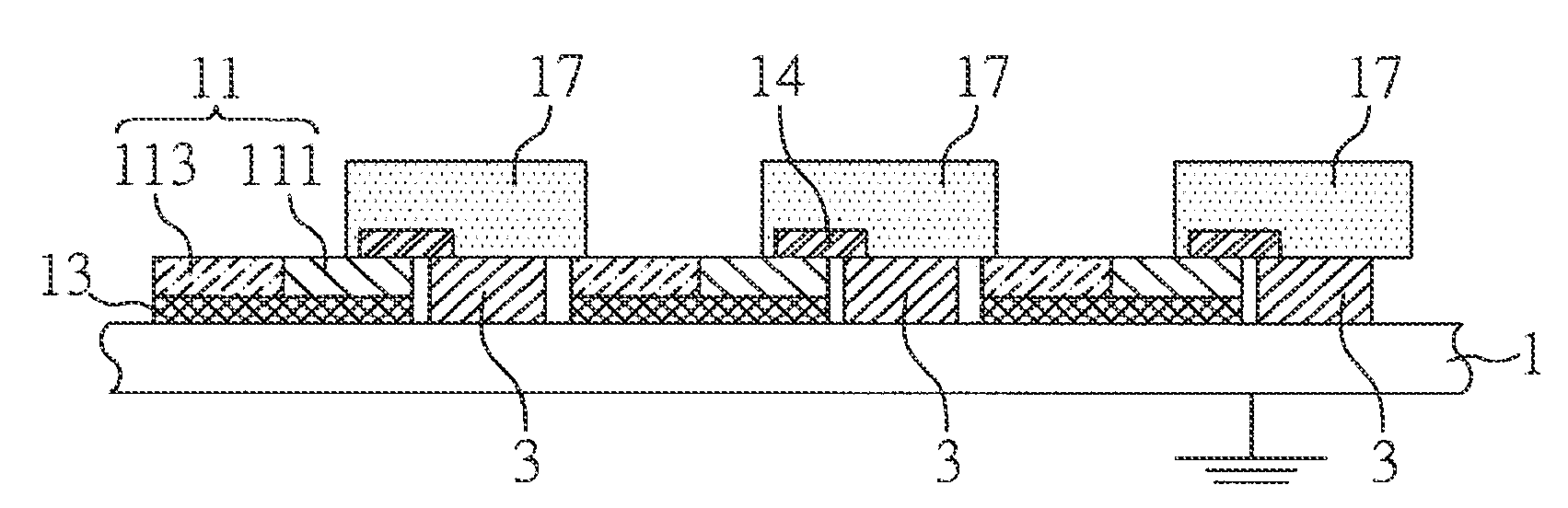
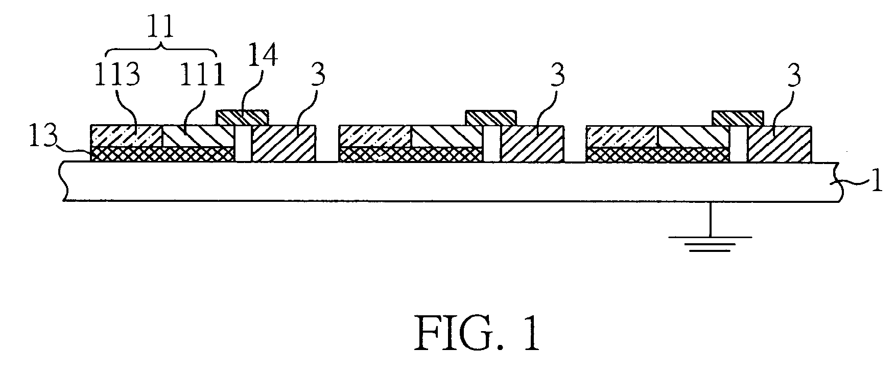
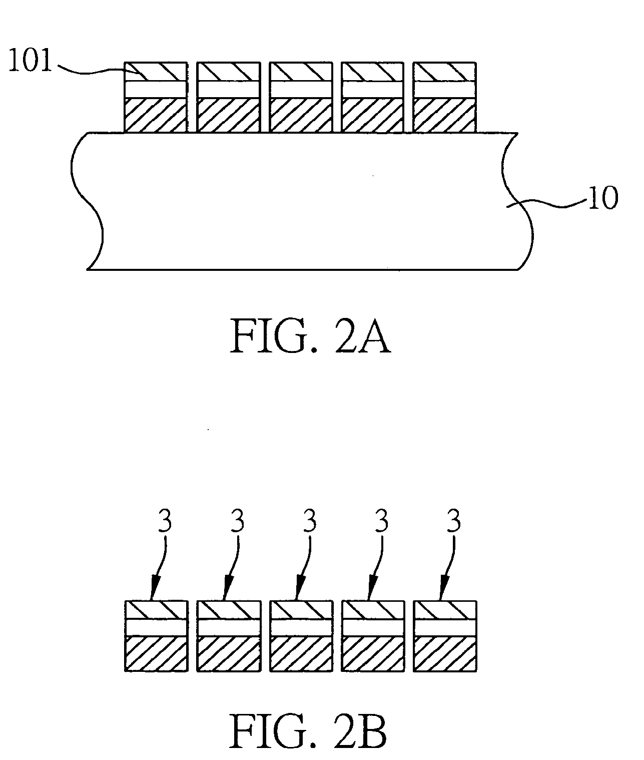
[0028]FIGS. 1 through 3B show a solid-state light emitting display and a fabrication method thereof according to a first embodiment of the present invention. Referring to FIG. 1, solid-state light emitting display of this embodiment at least comprises a metallic board 1 and a plurality of luminous microcrystals 3.

[0029]The metallic board 1 is preferably a flexible sheet, its thickness is, e.g., under 500 .mu.m, but it is not limited to this, e.g. it can also be an inflexible sheet. The metallic board 1 can be selected from stainless steel, such as number 304, 316, 430 aluminum alloy, such as series 2 to series 6, and plate that is made from other suitable metal, and the metallic board 1 has formed conductive circuitry 11 thereon. In this exemplary embodiment, the conductive circuitry 11 can be fabricated by the conventional IC (integrated circuit) fabricating process or other suitable fabricating process, so as to make the conductive circuitry 11 include a plurality of electrical co...

second embodiment

[0036]FIG. 4 shows a solid-state light emitting display and a fabrication method thereof according to a second embodiment of the present invention. The components identical or similar to the first exemplary embodiment is expressed as the same or similar component reference numbers, of which the detailed description is left out, in order to illustrate the present invention in a more clear and concise manner.

[0037]With reference to FIG. 4, the solid-state light emitting display comprises a metallic board 1 formed with a conductive circuitry, a plurality of luminous microcrystals 3 disposed on the surface of the metallic board 1 and electrically connecting with the conductive circuitry 11, and a fluorescent powder layers 17 at least respectively covering such luminous microcrystals 3. In the exemplary embodiment, such luminous microcrystals 3 can be, e.g., ultraviolet light emitting diode, or other suitable component, and the fluorescent powder layers 17 are formed by putting the fluor...


PUM


Abstract

A solid-state light emitting display and a fabrication method thereof are proposed. The light emitting display includes a metallic board formed with conductive circuits, and a plurality of luminous microcrystals disposed on a surface of the metallic board and electrically connected to the conductive circuits. The metallic board provides the features of lightness and thinness, and flexibility, and the luminous microcrystals are in the form of light emitting components, so as to improve the luminous efficiency of display and attain the effect of environmental protection and energy saving, thereby providing display technology with performance satisfactory for various display requirements.

Description

CROSS-REFERENCE TO RELATED APPLICATION[0001]This application is a divisional of copending application Ser. No. 11 / 295,504, filed Dec. 7, 2005, and the right of priority of parent application is and was claimed under 35 USC § 119 of Taiwanese Application No. 094116425, filed May 20, 2005, the entire disclosure of which is incorporated herein by reference.FIELD OF THE INVENTION[0002]The present invention relates to displays and fabrication methods thereof, and more particularly, to a solid-state light emitting display and a fabrication method thereof with a flat-panel display technology.BACKGROUND OF THE INVENTION[0003]In order to fulfil visual requirement and more information contained, the demand for the display size and resolution becomes more and more high, thus, the FDP (flat display panel) has become an important component part of electronic product. However, the characteristic of curtailing the display volume has not yet fulfilled the market requirement for the display hencefor...

Claims


Application Information

Patent Timeline
Patent Type & Authority Applications(United States)
IPC IPC(8): H01L21/00
CPCG09F9/30G09F9/33
Inventor HUNG, CHIA-HUNGCHANG, CHIA-CHIANGLIN, CHUN-HUNG
Owner IND TECH RES INST
Why Eureka
Try Eureka