Ultra Thin Channel (UTC) MOSFET Structure Formed on BOX Regions Having Different Depths and Different Thicknesses Beneath the UTC and SourceDrain Regions and Method of Manufacture Thereof

a mosfet and ultra-thin technology, applied in the direction of semiconductor devices, electrical devices, transistors, etc., can solve the problems of loss of performance due to inefficient transfer of stress to the channel, inability to manufacture, and undesirable thin boxes in soi cmos devices, etc., to reduce overlap capacitance, gate to, and eliminate variations in channel strain

Active Publication Date: 2008-11-20
GLOBALFOUNDRIES US INC
View PDF16 Cites 28 Cited by
  • Summary
  • Abstract
  • Description
  • Claims
  • Application Information

AI Technical Summary

Benefits of technology

[0014]The self-alignment eliminates variations in channel strain due to alignment tolerances between the Gate Conductor (GC) mask level and the RX mask level. The RX mask is used to define where transistors are to be formed. The GC mask is employed to define the location of the gate conductors. Note that when reference is made to the tolerance between GC and RX levels, reference is being made as to how precisely the gate conductor (GC) aligns to the edges of the regions containing the transistors (semiconductor-on-insulator body+source / drain regions.)
[0015]Furthermore, gate to diffusion overlap can now be minimized, resulting in reduced overlap capacitance and higher performance.
[0016]The embedded source-drain regions can now be placed much closer to the gate edge, resulting in reduced extrinsic source-drain resistance and higher performance.
[0017]The method uses a replacement gate process, which allows the use of a high-K / Metal gate dielectric for improved device scaling and reduced gate leakage.

Problems solved by technology

In addition thin BOX is undesirable in SOI CMOS devices because of electric field fringing in the BOX as described by V. P. Trivedi, et al entitled “Nanoscale FD / SOI CMOS: Thick or Thin BOX?” IEEE Electron Device Letters, Vol. 26, No. 1, (January 2005) pp.
Another problem with thin uniform BOX structures in CMOS devices is that the CMOS speed is reduced as stated by Trivedi in the above cited article.
Still another problem is encountered, particularly with semiconductor devices with Raised Source / Drain (RSD) and Ultra-Thin Channel (UTC) semiconductor-on-insulator devices, which is the requirement for low raised source-drain for resistance forces the stressed liners to be located farther away from the channel than would be desired by the designer.
The loss of performance due to the inefficient transfer of stress to the channel is compounded by the competing need to use sidewall insulating spacers which are as thick as possible, to minimize gate to source-drain capacitance.
There is another problem which is that dislocations in a silicon substrate are caused by oxygen ion implanted into that silicon substrate.
The embodiment of Hsu et al. is an example of the above described problem that it has high gate to source-drain capacitance and poor stress transfer to the channel.
To avoid high gate to source-drain capacitance very thick sidewall spacers are used, which results in very poor stress transfer if an overlying stress liner is used.
Chen et al. does not teach the use of porous silicon to form BOX regions.
The semiconductor under the gate is bulk and therefore suffers from the short channel scaling problems that our UTSOI structure solves.

Method used


Image

  • Ultra Thin Channel (UTC) MOSFET Structure Formed on BOX Regions Having Different Depths and Different Thicknesses Beneath the UTC and SourceDrain Regions and Method of Manufacture Thereof
  • Ultra Thin Channel (UTC) MOSFET Structure Formed on BOX Regions Having Different Depths and Different Thicknesses Beneath the UTC and SourceDrain Regions and Method of Manufacture Thereof
  • Ultra Thin Channel (UTC) MOSFET Structure Formed on BOX Regions Having Different Depths and Different Thicknesses Beneath the UTC and SourceDrain Regions and Method of Manufacture Thereof

Examples


Embodiment Construction

[0029]The method of this invention provides for fabrication of a UT or a UT semiconductor-on-insulator MOSFET with high-K / metal self-aligned replacement gate and embedded source / drains using oxidized porous silicon, described below with reference to the FIGS. 1A-1W, 2 and 3.

UTC SEMOI MOSFET Embodiment and a Method of Formation Thereof

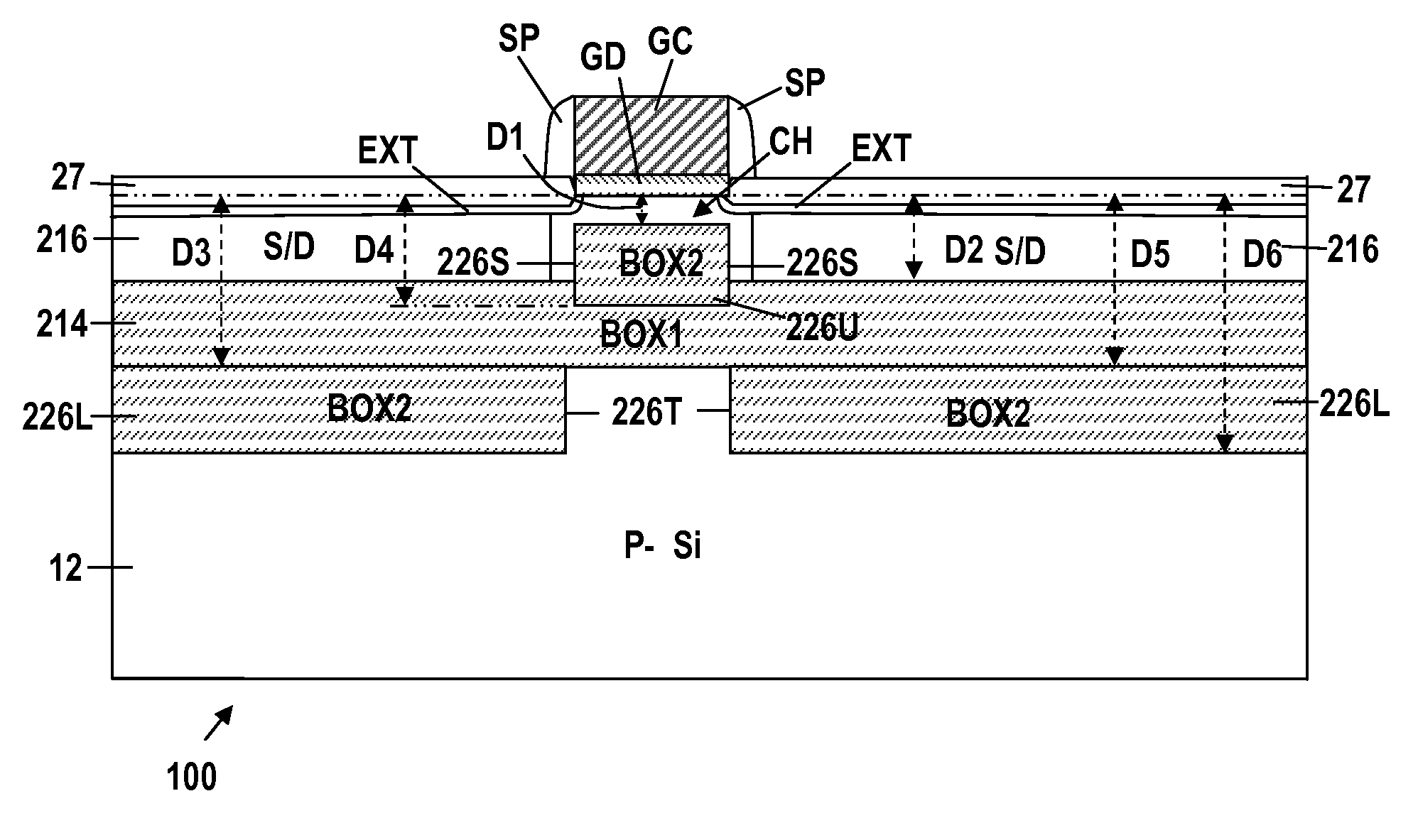
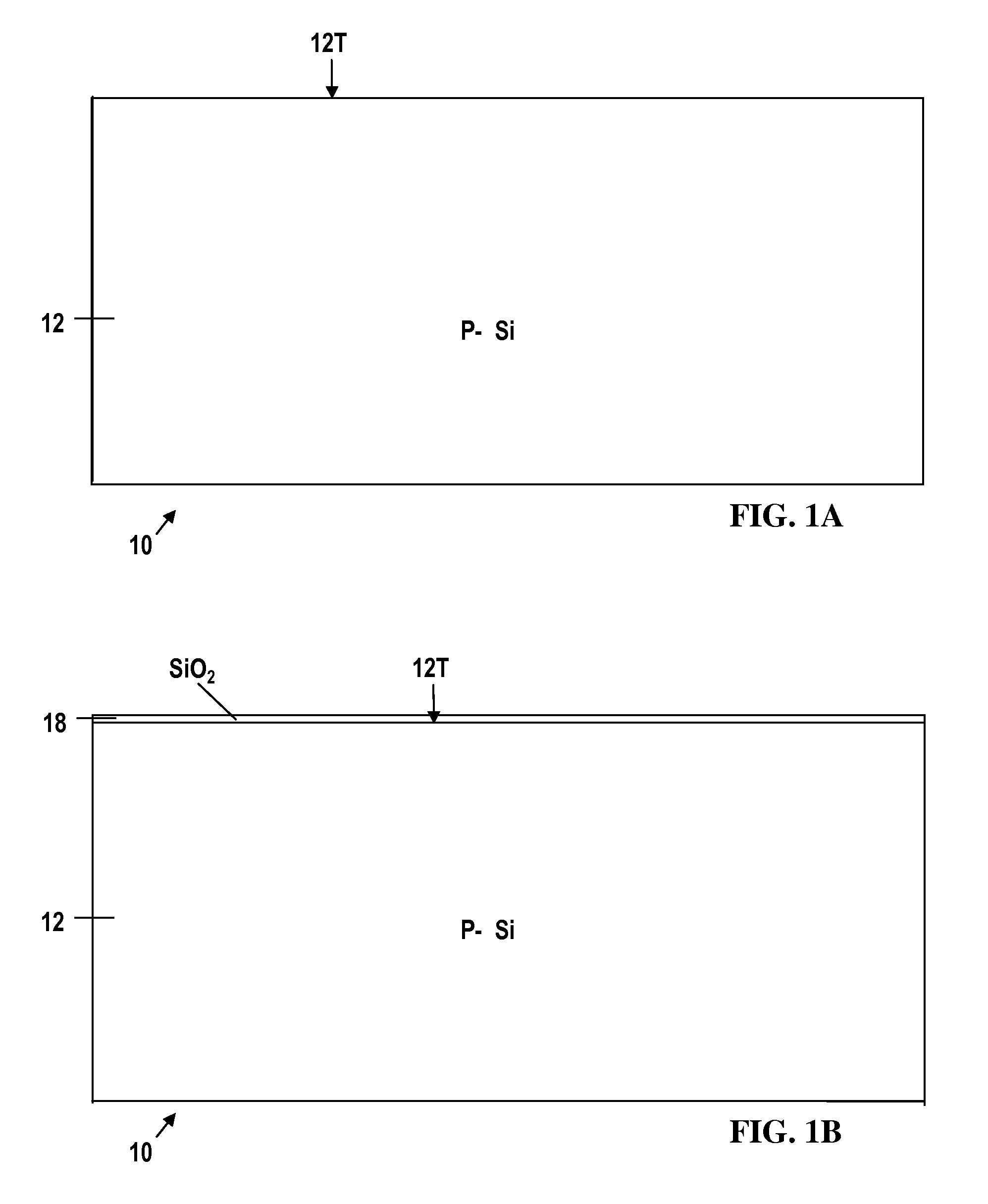
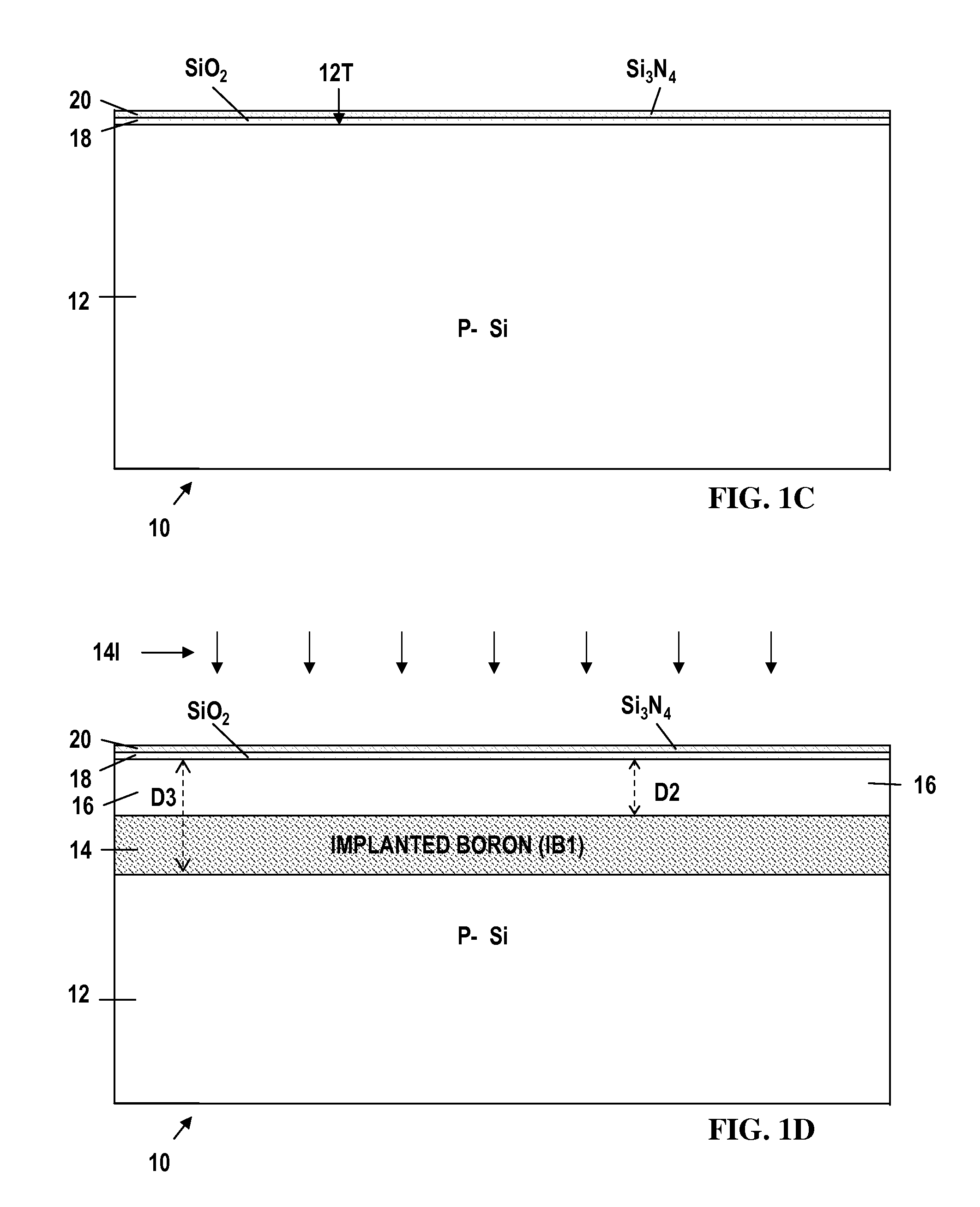
[0030]FIG. 1A shows a sectional view of a device 10 in accordance with this invention in an early stage of fabrication of a UTC SEMOI MOSFET starting in accordance with step A of FIG. 3. The method begins preferably with a bulk substrate 12 which is to be the substrate upon which a SEMOI structure is to be formed. An insulator in the form of a Buried OXide (BOX) layer will be formed on or in the bulk substrate 12 at some point in the process. The SEMOI structure will be a semiconductor layer formed on an insulator which is formed on the bulk substrate 12. Heretofore the most commonly used SEMOI structures have employed Silicon (Si) as the semiconductor ...


PUM


Abstract

A MOSFET structure includes a planar semiconductor substrate, a gate dielectric and a gate. A UT SOI channel extends to a first depth below the top surface of the substrate and is self-aligned to and is laterally coextensive with the gate. Source-drain regions, extend to a second depth greater than the first depth below the top surface, and are self-aligned to the UT channel region. A BOX1 region extends across the entire structure, and vertically from the second depth to a third depth below the top surface. An upper portion of a BOX2 region under the UT channel region is self-aligned to and is laterally coextensive with the gate, and extends vertically from the first depth to a third depth below the top surface, and where the third depth is greater than the second depth.

Description

[0001]This application is a continuation-in-part of copending U.S. patent application Ser. No. 11 / 162,959, filed 29 Sep. 2005 entitled “Planar Ultra-Thin Semiconductor-On-Insulator Channel MOSFET with Embedded Source / Drain.”BACKGROUND OF THE INVENTION[0002]This invention relates to Ultra Thin (UT) Metal Oxide FET (MOSFET) devices. While the embodiment comprises a MOSFET device, as indicated by the title, the present invention can be embodied in Metal Insulator FET (MISFET) devices which employ gate dielectrics other than oxides. The term Ultra Thin (UT), as employed herein refers to Ultra Thin Channel (UTC) regions in SEMiconductor-On-Insulator (SEMOI) FET devices with the source and drain regions formed in thicker SEMOI or Silicon-On-Insulator (SOI) regions of a semiconductor substrate aside from the UTC regions. As employed herein the term SEMiconductor-On-Insulator (SEMOI) is a generic term which refers generally to structures of a semiconductor layer formed on an insulator such ...

Claims


Application Information

Patent Timeline
Patent Type & Authority Applications(United States)
IPC IPC(8): H01L29/786H01L21/336
CPCH01L21/2652H01L21/3003H01L29/1083H01L29/66545H01L29/6659H01L29/66772H01L29/7833H01L29/78603H01L29/78621H01L29/78696
Inventor CHENG, KANGGUOCHIDAMBARRAO, DURESETIGREENE, BRIAN JOSEPHMANDELMAN, JACK A.RIM, KERN
Owner GLOBALFOUNDRIES US INC
Why Eureka
Try Eureka