Semiconductor package with through silicon via and related method of fabrication

a technology of silicon via and semiconductor, applied in the direction of semiconductor devices, semiconductor/solid-state device details, electrical apparatus, etc., can solve the problems of limiting the degree to which ic packages can be miniaturized, complicated bonding process of forming bga packages, undetectable interconnection technologies of ic packages, etc., to achieve the effect of improving electrical interconnections

Inactive Publication Date: 2008-11-20
SAMSUNG ELECTRONICS CO LTD
View PDF10 Cites 188 Cited by
  • Summary
  • Abstract
  • Description
  • Claims
  • Application Information

AI Technical Summary

Benefits of technology

[0013]In order to provide IC packages with improved electrical interconnections, as compared with conventional IC packages, selected embodiments of the invention include IC packages and r

Problems solved by technology

Unfortunately, most of these conventional interconnection technologies for IC packages are either undesirably complicated or they tend to limit the degree to which the IC packages

Method used


Image

  • Semiconductor package with through silicon via and related method of fabrication
  • Semiconductor package with through silicon via and related method of fabrication
  • Semiconductor package with through silicon via and related method of fabrication

Examples


Embodiment Construction

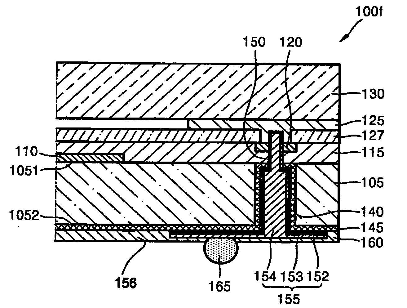
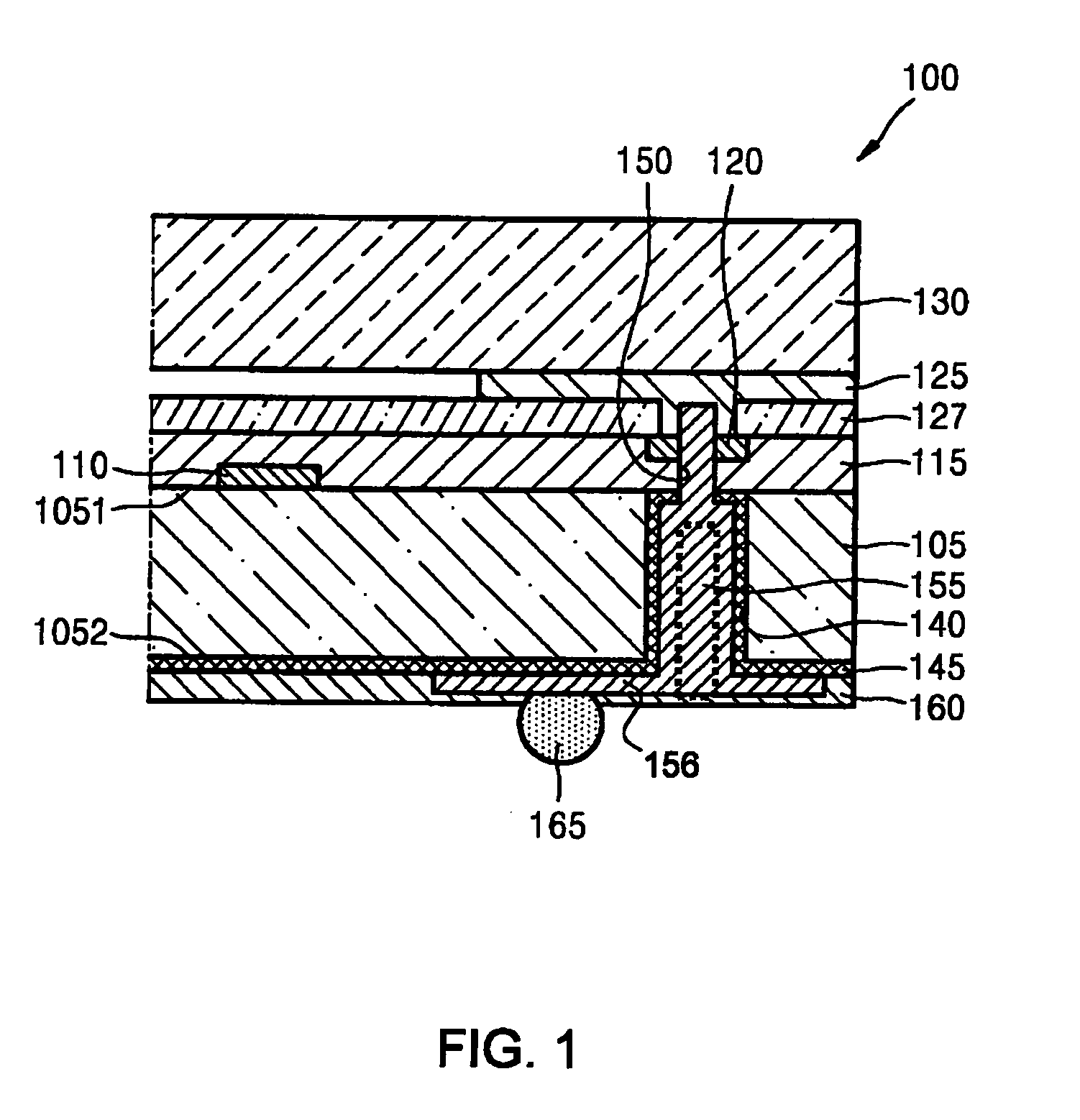
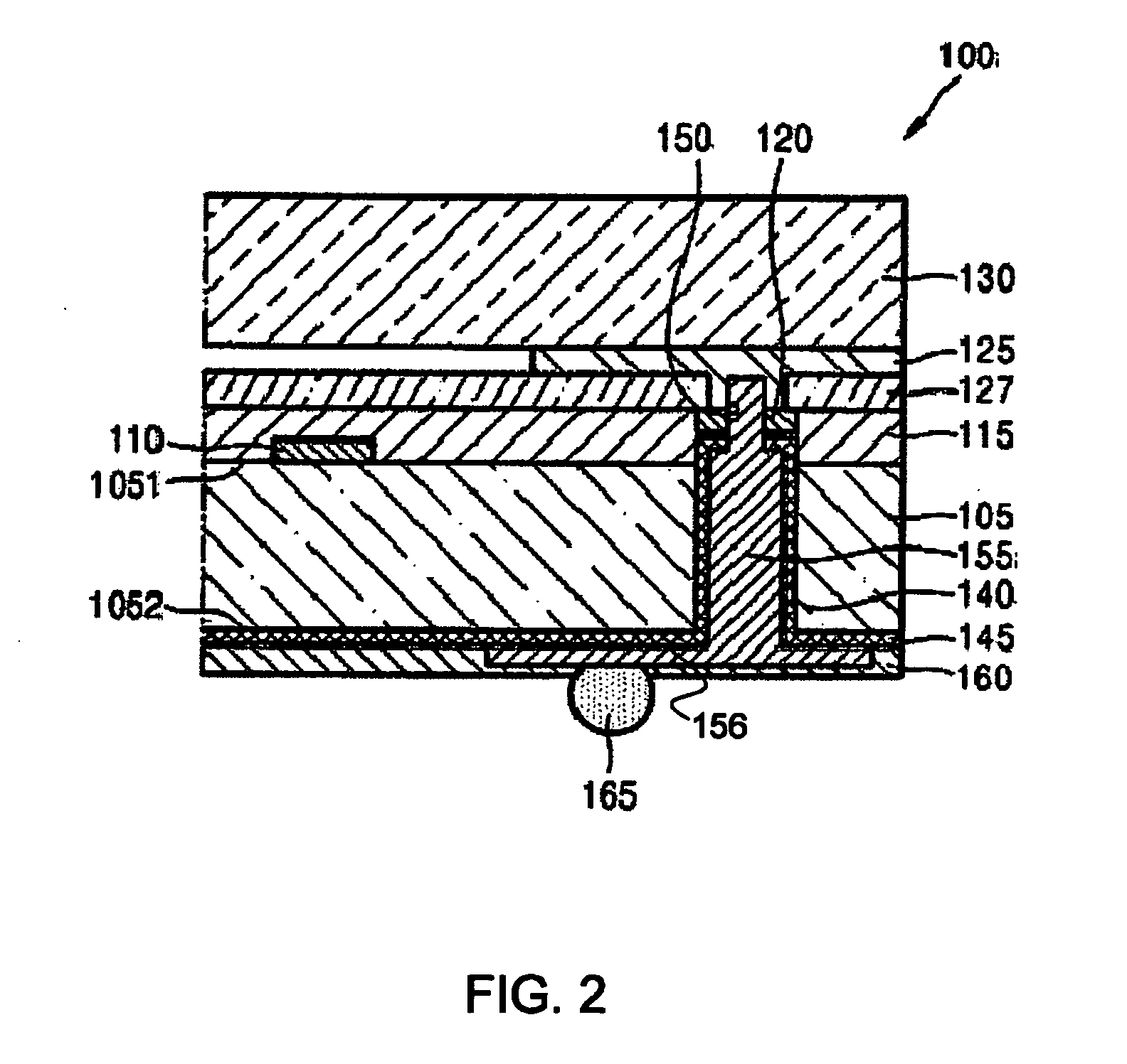
[0025]Embodiments of the invention are described below with reference to the corresponding drawings. These embodiments are presented as teaching examples while the actual scope of the invention is defined by the claims that follow.

[0026]FIGS. 1 through 10 are schematic diagrams variously illustrating a semiconductor package 100 in accordance with selected embodiments of the invention. Semiconductor package 100 may be used to implement a semiconductor device such as a dynamic random access memory (DRAM), a static random access memory (SRAM), a non-volatile memory such as a flash memory, or an active pixel sensor (e.g., a complementary metal-oxide semiconductor (CMOS) image sensor), etc.

[0027]Referring to FIG. 1, semiconductor package 100 comprises a semiconductor substrate 105 having a first (upper) surface 1051 and a second (lower) surface 1052. Semiconductor substrate 105 may be conventionally formed from a silicon (Si) wafer, a germanium (Ge) wafer, and / or a silicon-germanium (SiG...


PUM


Abstract

In a semiconductor package, an electrode has a first part extending through a semiconductor substrate and a second part extending from the first part through a compositional layer to reach a conductive pad.

Description

CROSS-REFERENCE TO RELATED APPLICATIONS[0001]This application claims priority to Korean Patent Applications. 10-2007-0048911 filed on May 18, 2007 and 10-2007-0123811 fitted Nov. 30, 2007, the collective subject matter of which is hereby incorporated by reference.BACKGROUND OF THE INVENTION[0002]1. Field of the Invention[0003]The invention relates generally to semiconductor integrated circuit (IC) packages. More particularly, the invention relates to semiconductor IC packages including a through silicon via and related electrode, as well as methods of fabricating same.[0004]2. Description of Related Art[0005]Modern electronic devices rely on integrated circuit (IC) technology to provide a wide variety of functionality, including, for example, data storage, data processing, signal amplification, signal transduction, and so on. Some common examples of IC technology providing this functionality include memory chips and microprocessors used in personal computers and portable electronic ...

Claims


Application Information

Patent Timeline
IPC IPC(8): H01L23/48
CPCH01L21/76898H01L2224/0401H01L27/14618H01L27/14625H01L31/0203H01L2924/01077H01L2924/14H01L2224/05H01L2224/02372H01L2224/05548H01L2224/06181H01L2224/13H01L2224/13022H01L2224/13024H01L23/481
Inventor JANG, HYUNG-SUNKANG, UN-BYOUNGKWON, WOON-SEONGKWON, YOUNG-CHAILEE, CHUNG-SUNLEE, DONG-HO
Owner SAMSUNG ELECTRONICS CO LTD
Why Eureka
Try Eureka