

A/D converter circuit and A/D conversion method
a converter circuit and converter technology, applied in the field of a/d converter circuit and a/d conversion method, can solve the problems of repetitive operation, large scale of arithmetic processing circuit, and inability to meet high-speed a/d conversion processing technology, etc., to achieve the effect of improving linearity in the output of a/d conversion
- Summary
- Abstract
- Description
- Claims
- Application Information
AI Technical Summary
Benefits of technology
Problems solved by technology
Method used
Image

Examples
first embodiment
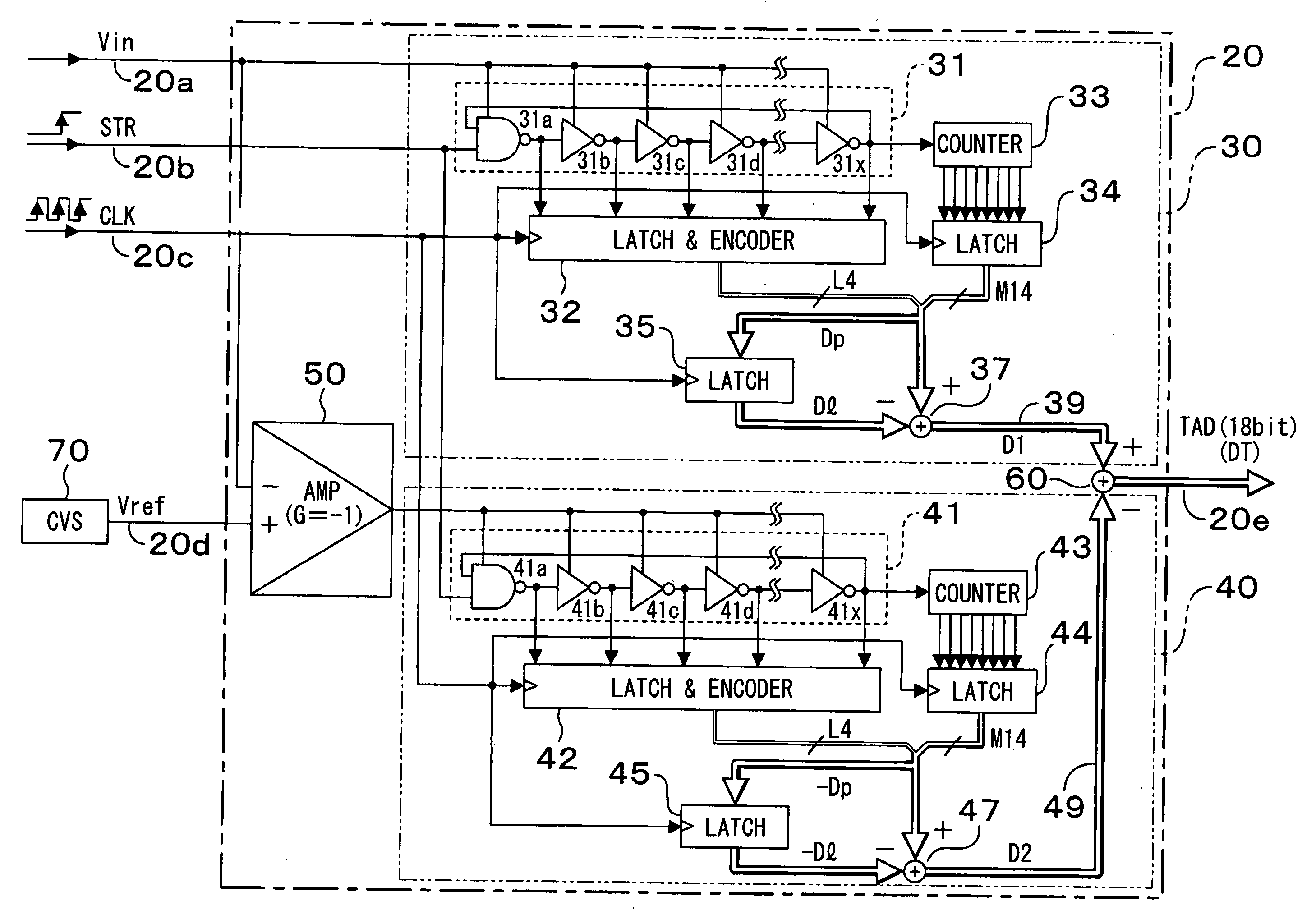
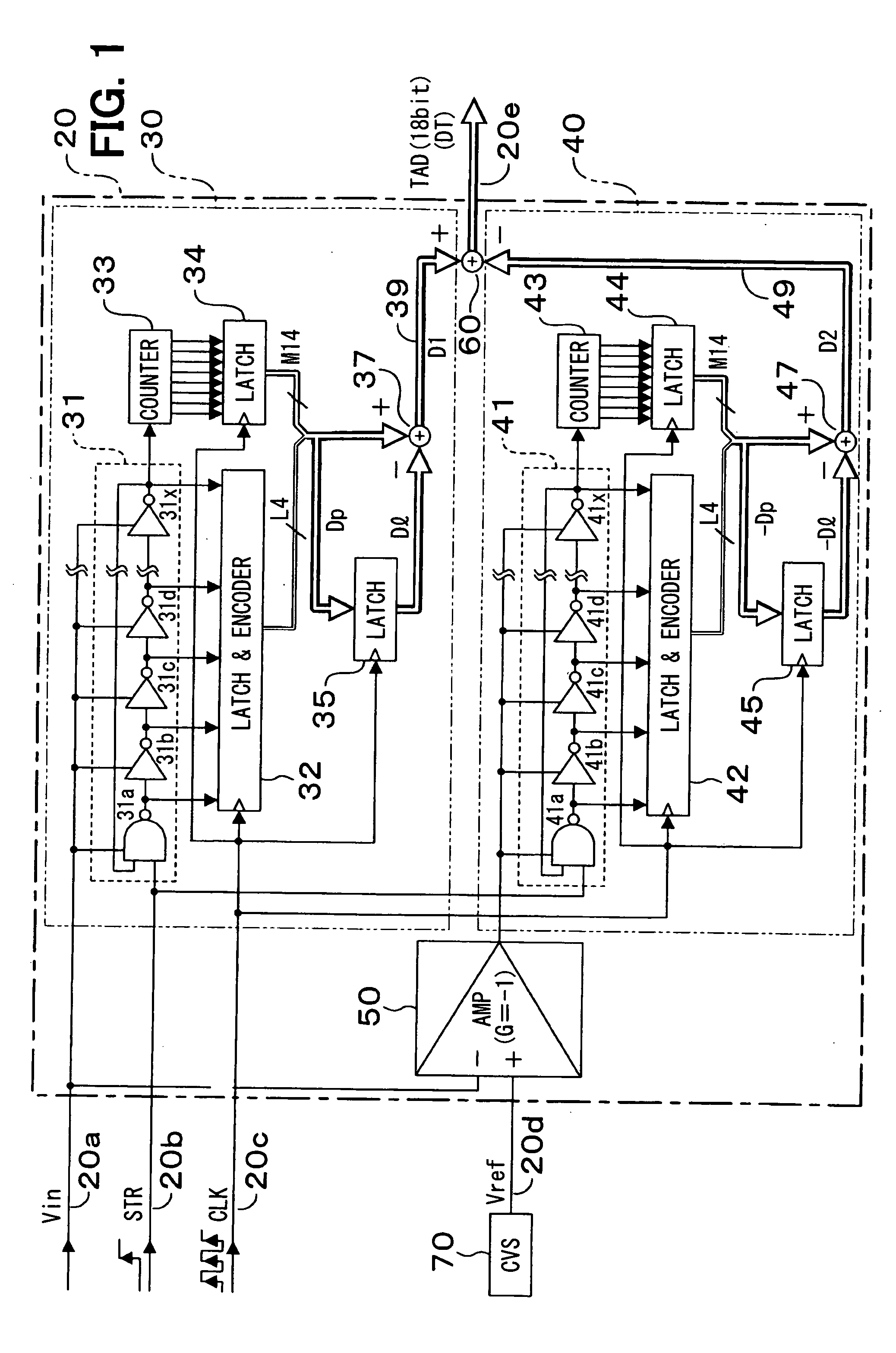
[0026]Referring first to FIG. 1, an A / D converter circuit 20 is configured by a first converter unit 30, a second converter unit 40 and an inverting amplifier 50, and operates to convert an analog input voltage Vin input to an input line 20a into a binary digital data DT and to output it to an output line 20e.
[0027]The first converter unit 30 converts the analog input voltage Vin input to the input line 20a into a binary first digital data and outputs it to a first conversion output line 39, and is configured by a first ring delay line 31, a first latch and encoder 32, a first counter 33, latches 34 and 35, and a digital arithmetic circuit 37. The first converter unit 30, as will be described below, utilizes the fact that the inverting operation time of the inverting circuits in the first ring delay line 31 differs depending upon the input voltage Vin.
[0028]Here, as will be described later, the first digital data D1 output to the first conversion output line 39 is produced by subtr...
second embodiment
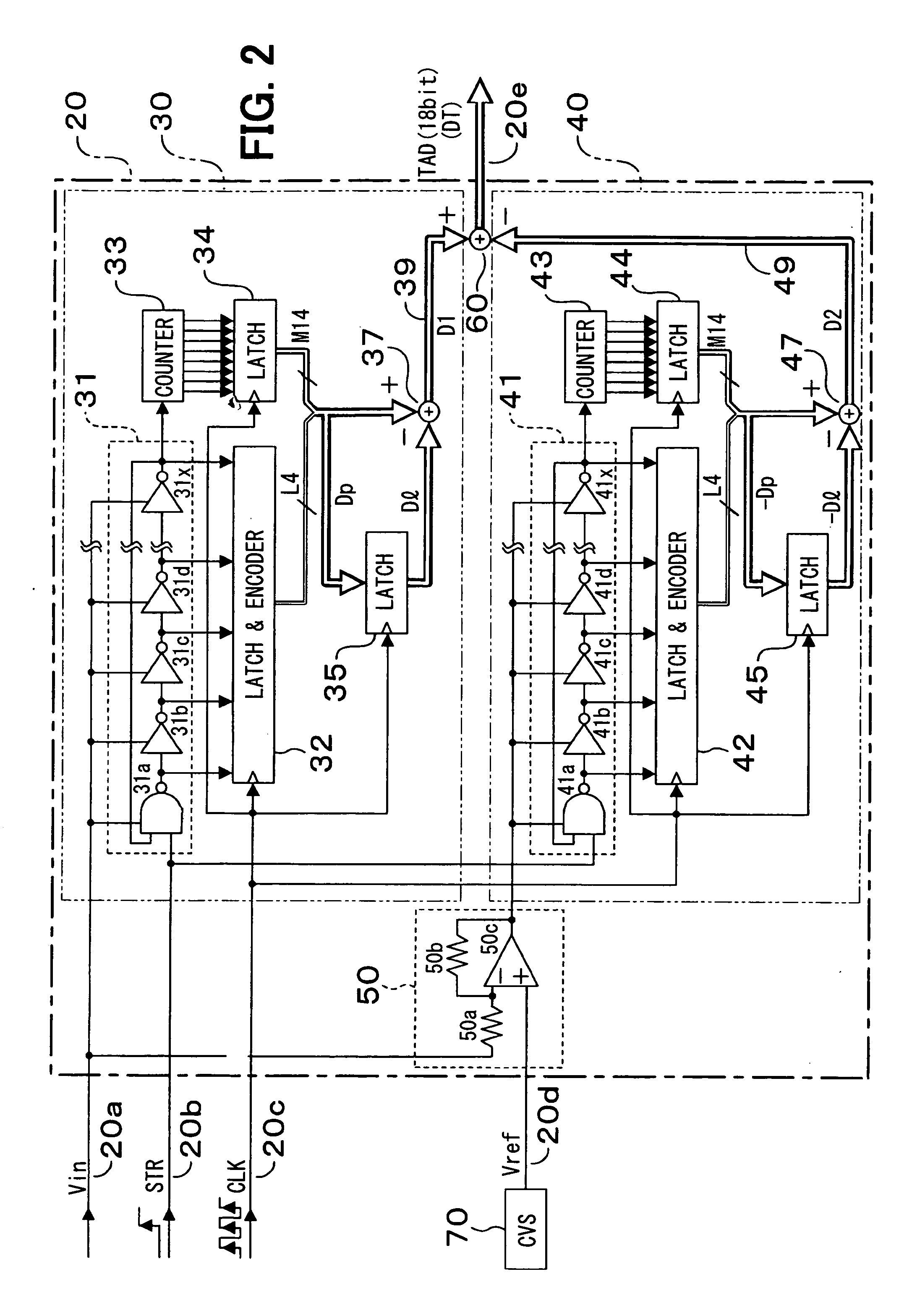
[0056]According to a second embodiment, an A / D converter circuit 120 is different from the first embodiment with respect to that the second converter unit 40 is simplified. Therefore, the constituent portions substantially the same as those of the A / D converter circuit 20 of the first embodiment are denoted by the same reference numerals.
[0057]The A / D converter circuit 120 is configured by the first ring delay line 31, first latch and encoder 32, first counter 33, latches 34, 35, 36 and 45, digital arithmetic circuits 37, 47 and 60, inverting amplifier 50, sampling and holding circuit 52, multiplexer 62 and control circuit 64. Here, the first ring delay line 31 operates as a pulse circulating circuit, the first counter 33 operates as a counter, the latch 35 operates as a first latch, the latch 36 operates as a 1′-st latch, the digital arithmetic circuit 37 operates as a first operation means, the latch 45 operates as a second latch, the digital arithmetic circuit 47 operates as a se...
third embodiment
[0070]According to a third embodiment shown in FIG. 8, an A / D converter circuit 220 is different from the first embodiment with respect to suppressing the variation in the digital data caused by a change in the ambient temperature.
[0071]In the A / D converter circuits 20 and 120 of the first and second embodiments described above, the first ring delay line 31 and the second ring delay line 41 are assumed to be configured by semiconductors such as MOS transistors. Therefore, the inverting operation time (delay time) varies depending upon the temperature due to their characteristics. Therefore, the output data value converted into the digital data based on the input voltage Vin input, as a power supply voltage, to the first ring delay line 31, could vary even depending upon a change in the ambient temperature. Therefore, the A / D converter circuit 220 of this embodiment improves the above point. Here, the constituent portions substantially the same as those of the A / D converter circuit 2...
PUM
 Abstract
Description
Claims
Application Information