Liquid crystal panel for liquid crystal display device

a liquid crystal display device and liquid crystal panel technology, applied in the field of liquid crystal panels, can solve the problems of uniform peripheral portion of the liquid crystal panel, insufficient large space at the peripheral area of the pixel region, waste of space, etc., and achieve the effect of decreasing the frame of the display device and increasing the width of the metal wiring

Active Publication Date: 2008-11-20
INFOVISION OPTOELECTRONICS HLDG LTD
View PDF2 Cites 20 Cited by
  • Summary
  • Abstract
  • Description
  • Claims
  • Application Information

AI Technical Summary

Benefits of technology

[0043]in said outer region, the wiring width of said metal wiring in the outer region is adjusted to allow the solidify, which is obtained by curing the seal material in the outer region by using the UV light curing, to be about 10%, so that the expansion of the uncured seal material during the heat-curing will not exceed the cut-off line used for cutting the liquid crystal panel off from the mother glass.
[0044]When the invention is used, the problem caused by “the UV light is masked by the metal wiring on the TFT substrate thereby part of the seal material cannot be cured” occurring in a condition that the seal material and BM are superposed and the UV light is irradiated from one side of the TFT substrate can be solved by irradiating effectively according to the seal material region, that is, a desired amount of UV light is irradiated to the region where the irradiation is required, and the width of the metal wiring can be increased in the region where the irradiation is not very required, thereby the drop of the resistance value of the metal wiring can be restricted generally to a specific range. As a result, the seal material and BM can be superposed, and the peripheral area of the panel can be used effectively, and the requirement for decreasing the frame of the display device in recent years can be reached.

Problems solved by technology

However, in case the seal material is disposed at the outer side of BM, then sufficient large space is required at the peripheral area of the pixel region.
As a result, the space is wasted.
Once the temperature at the places where the UV cure seal material under an uncured state contacting the liquid crystal rises during the following heat-cure process, the pollution substance is easy to be separated out from the seal material which has not been heat-cured to the liquid crystal, thereby the peripheral portion of the liquid crystal panel will be un-uniform.
The disadvantage under the condition of FIG. 6 is that the resistance of the wiring at the narrowed portion becomes larger, and the current value is limited when the voltage is applied, and the voltage drop produced by the resistance will be larger so that the desired voltage value cannot be obtained.
The disadvantage under the condition of FIG. 7 is that the Ohm connection of low resistance is required to be formed at the connection section for the contact hole connecting the metal wiring and the transparent electrode, however, a amount of current flows through said connection section, so that it is difficult to form a highly reliable Ohm connection corresponding to said current.
The disadvantage under the condition of FIG. 8 is that the resistance of the wiring portion forming the slot becomes larger, the current is limited when the voltage is applied, or the voltage drop becomes larger because of the resistance, therefore the problem that the desired voltage value cannot be obtained comes up.
Furthermore, another countermeasure beyond those described above is a kind of design in which the metal wiring and the seal material are not superposed, however, under such condition, the metal wiring is disposed at the peripheral area so that the purpose of utilizing effectively the peripheral space cannot be reached.

Method used


Image

  • Liquid crystal panel for liquid crystal display device
  • Liquid crystal panel for liquid crystal display device
  • Liquid crystal panel for liquid crystal display device

Examples


Embodiment Construction

[0085]The embodiments of the invention will be described with reference to the drawings as follows.

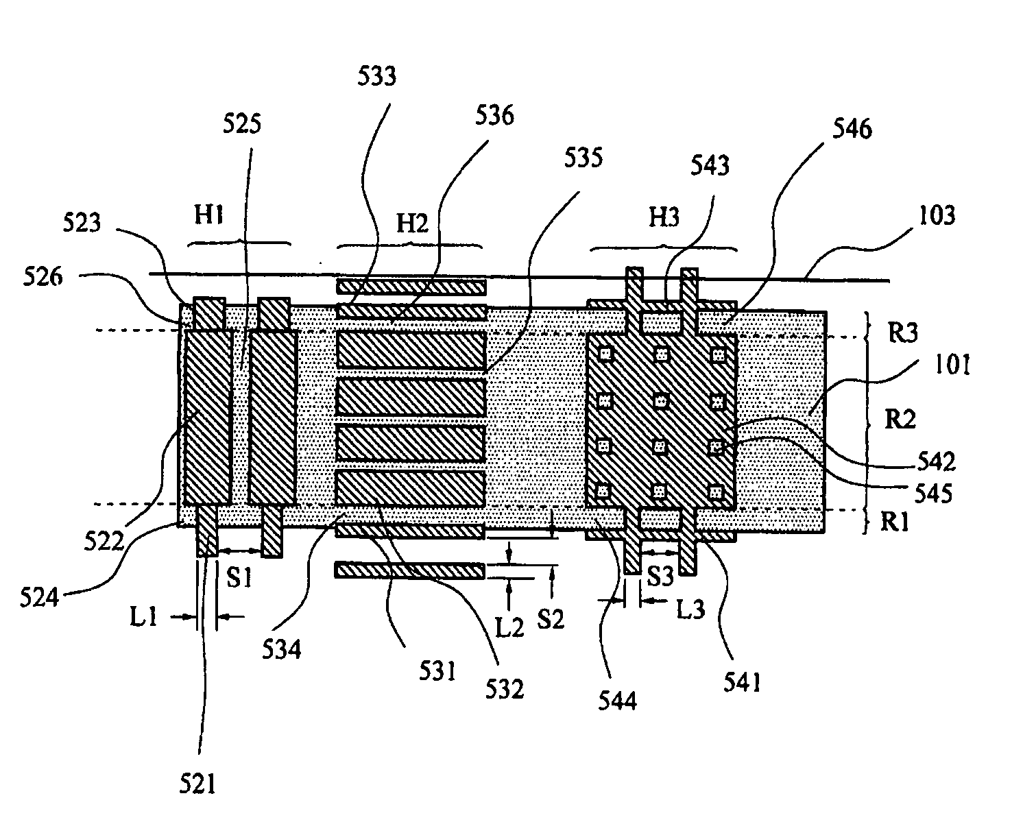
[0086]FIG. 5 is a plan view describing conceptually the wiring structure of a liquid crystal panel according to an embodiment of the invention. In FIG. 5, 101 is a seal material, 103 is a cut-off line of the substrate, R1 is an adjacent region of the seal material, R2 is a middle region of the seal material, R3 is an outer region of the seal material, H1 is a wiring structure when the metal wiring and the seal material are intersected, H2 is a wiring structure when the metal wiring and the seal material are disposed in parallel, H3 is a wiring structure when the metal wiring and the seal material are superposed, 521 is metal wiring in the adjacent region under the condition of the wiring structure of H1, 522 is metal wiring in the middle region under the condition of the wiring structure of H1, 523 is metal wiring in the outer region under the condition of the wiring structure of H1, 5...


PUM

PropertyMeasurementUnit
widthaaaaaaaaaa
widthaaaaaaaaaa
widthaaaaaaaaaa

Abstract

To utilize effectively the panel space of the liquid crystal panel, this invention has provided a wiring structure, in which the seal material and BM are coated in a superposition and the UV light is irradiated from one side of the TFT substrate; this invention has also provided a wiring structure, in which the seal material can still be irradiated by the UV light with high efficiency, meanwhile, the drop of the resistance value of the metal wiring on the TFT substrate can be restricted to a specific range. The solution is: the liquid crystal dropped is sandwiched between the TFT substrate and the CF substrate, meanwhile the liquid crystal panel is formed by adhering the light cured seal material disposed at the peripheral area of two substrates. In the adhering-formed liquid crystal panel, for the wiring portion, which is the portion of wiring disposed on the TFT substrate superposing the light cured seal material, the wiring structure is formed as follows, that is, the region of the seal material is divided into three regions, an adjacent region, a middle region and an outer region. The function of the respective regions must be held, and the resistance of the metal wiring is minimized under the precondition that the respective function is satisfied sufficiently.

Description

FIELD OF THE INVENTION[0001]The invention relates to a liquid crystal panel for an active matrix liquid crystal display device.DESCRIPTION OF THE RELATED ART[0002]In recent years, Thin Film Transistor-Liquid Crystal Display (TFT-LCD) panel has been used widely as the monitor of the desktop personal computer and the display device of the notebook computer. For the future, besides that TFT-LCD should satisfy the performances required for operating as a display device, from the viewpoint of decreasing the costs, it is important to improve the production efficiency by using larger mother glass substrate and to enhance the producing effects of the batch production by generalizing the components to reduce the manufacturing costs.[0003]Therefore, as an indispensable manufacturing method for increasing the production efficiency, the number of LCD panels that can be arranged here is an important parameter relating directly to the throughput in a method referred to as “multiple-sheet-cutting”...

Claims


Application Information

Patent Timeline
Patent Type & Authority Applications(United States)
IPC IPC(8): G02F1/1339G02F1/1343
CPCG02F1/133351G02F1/1339G02F1/1345G02F1/136286G02F2202/023
Inventor KAMIYA, HIROYUKICHENG, HSIN-ANTING, C.P.
Owner INFOVISION OPTOELECTRONICS HLDG LTD
Why Eureka
Try Eureka