Method for kinetically controlled etching of copper

a technology of kinetic control and etching, which is applied in the direction of metallic image processing, instruments, photomechanical equipment, etc., can solve the problems of limiting the use of electronic devices, affecting the performance or reliability of electronic devices, and low etching rate that cannot easily meet manufacturing throughput requirements, etc., and achieves simple and inexpensive processing conditions.

Inactive Publication Date: 2008-11-20
IBM CORP
View PDF33 Cites 32 Cited by
  • Summary
  • Abstract
  • Description
  • Claims
  • Application Information

AI Technical Summary

Benefits of technology

[0026]A remarkable feature of the etching process is that the etching rate is only weakly dependent on flow conditions near the substrate surface. Consequently, as described in more detail below, a wide range of flow rates cor

Problems solved by technology

Any anisotropic etching of the copper or roughening of the copper surface may significantly degrade the performance or reliability of the electronic device.
Generally, etchants (etching compositions or solutions) are either intrinsically anisotropic, or have low etch ra

Method used


Image

  • Method for kinetically controlled etching of copper
  • Method for kinetically controlled etching of copper
  • Method for kinetically controlled etching of copper

Examples


examples

[0061]The following non-limiting examples are presented to further illustrate the etchants and etching processes of the disclosure.

Etchant A

[0062]An etchant was prepared containing the following: 0.05 molar (M) alanine, 1.0 M hydrogen peroxide, 0.02 M phosphate buffer at pH 7.44, and 0.05 wt % CDTA. A 200 mm patterned wafer of a CMOS structure was etched in a rotating single-wafer immersion tool with rotation rate of 50 rpm.

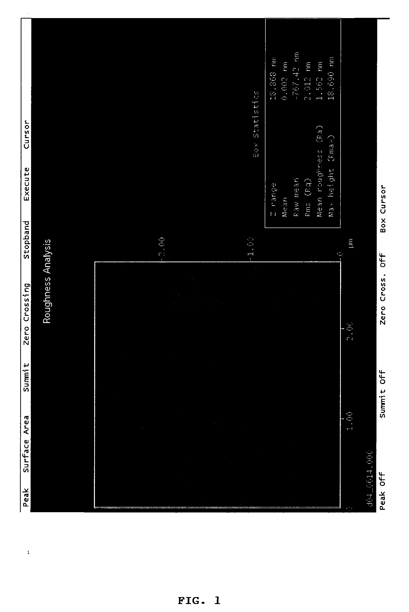
[0063]An atomic force microscope (AFM) image of the copper (Cu) surface after a 100 nm etch of the patterned CMOS structure is shown in FIG. 1. The copper surface roughness before etching was about 1 nm RMS, and after 100 nm etch was about 2 nm RMS.

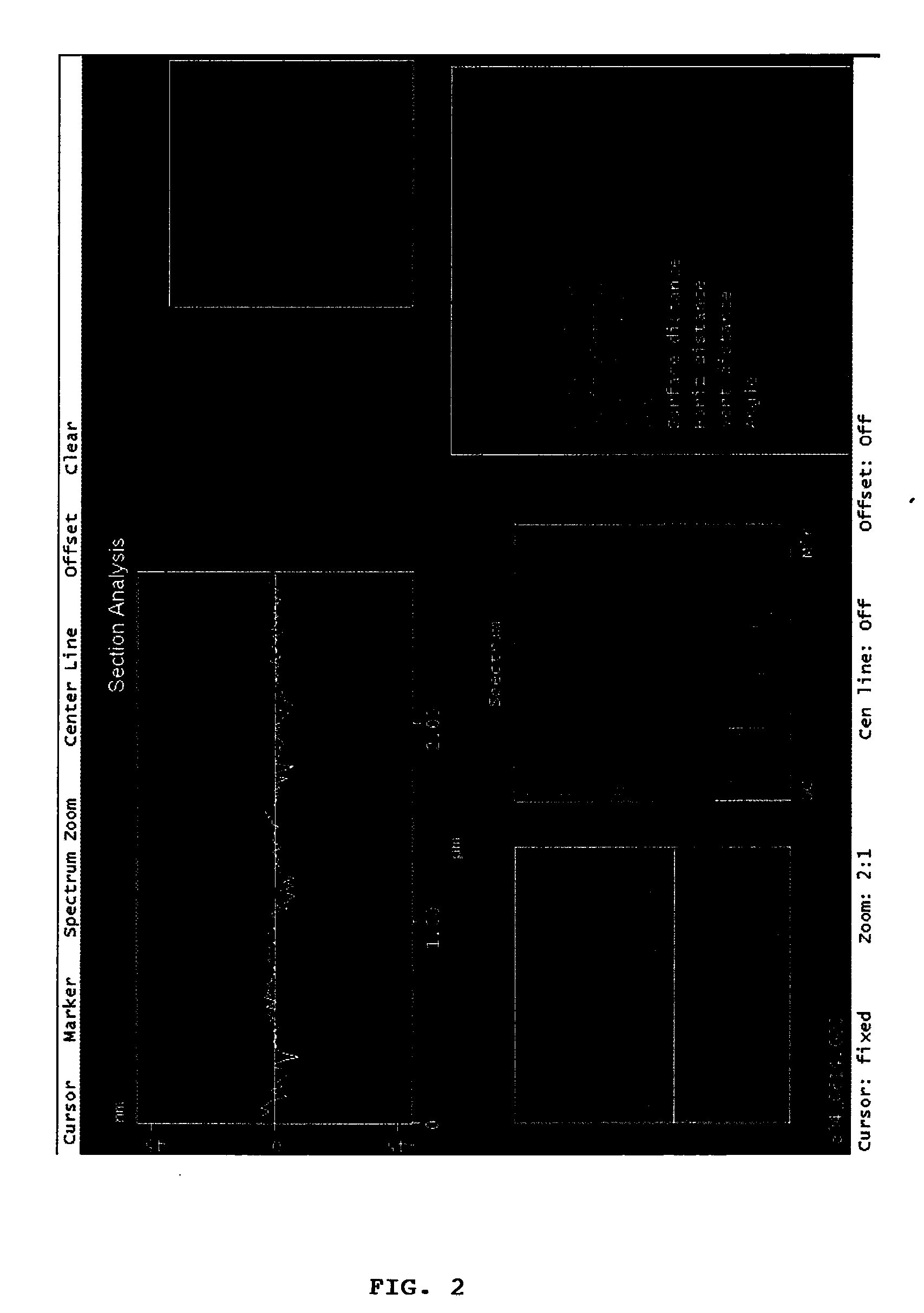
[0064]FIG. 2 shows an AFM line scan of the etched Cu of FIG. 1. In particular, the image shows maximum Cu height difference of about 6 nm across grains after 100 nm etch of the patterned CMOS structure.

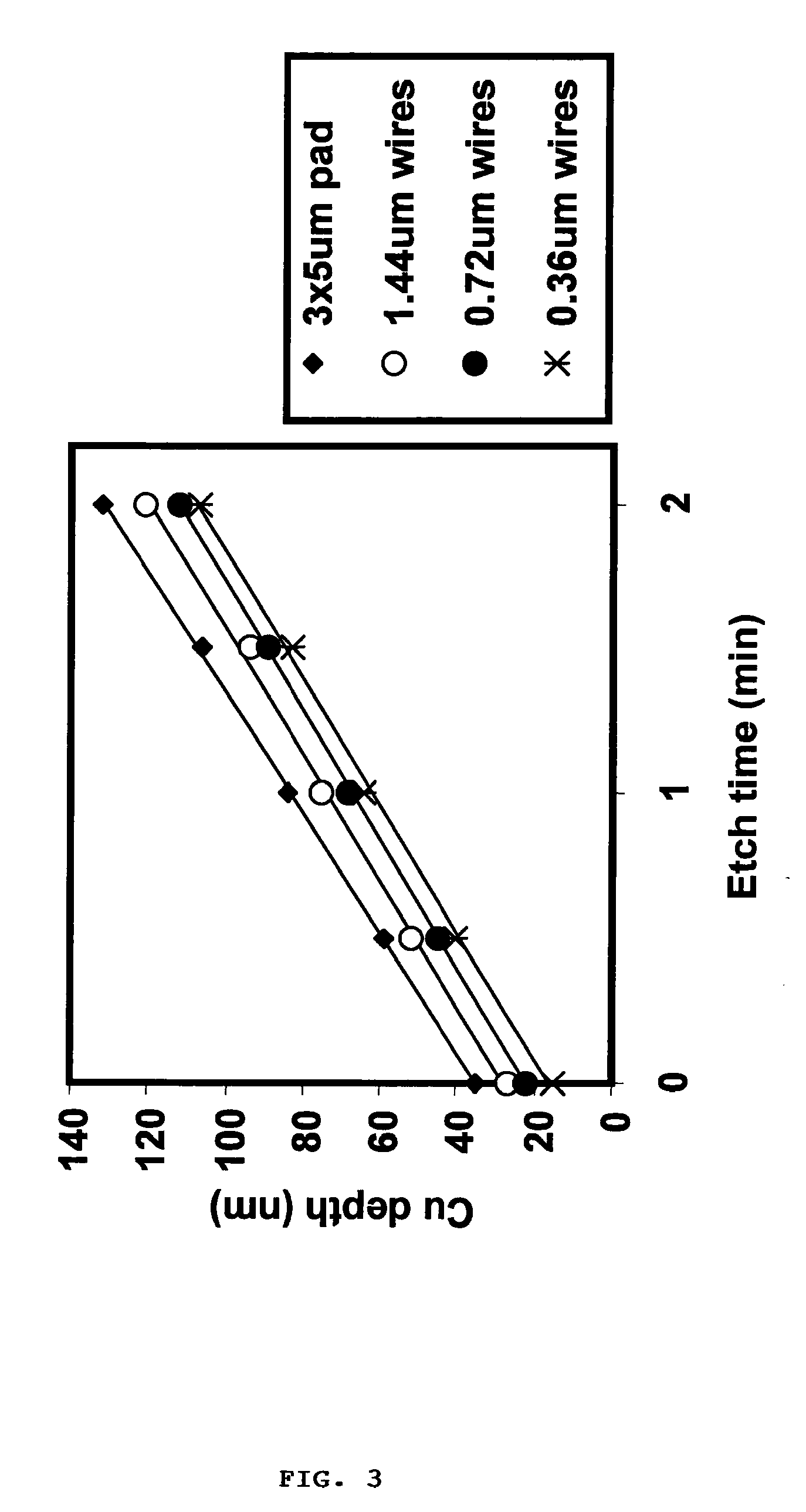
[0065]FIG. 3 shows a plot of AFM-measured Cu depths after timed etches of patterned CMOS wafers. In particular, the fe...


PUM

PropertyMeasurementUnit
Temperatureaaaaaaaaaa
Thicknessaaaaaaaaaa

Abstract

An etching composition, particularly for kinetically controlled etching of copper and copper alloy surfaces; a process for etching copper and copper alloys, particularly for etching at high rates to provide uniform and smooth, isotropic surfaces; an etched copper or copper alloy surface obtained by the process; and a process for generating copper or copper alloy electrical interconnects or contact pads. The etching composition and etching processes provide a smooth, isotropic fast etch of copper and copper alloys for semiconductor fabrication and packaging.

Description

BACKGROUND[0001]1. Technical Field[0002]The disclosure relates to an etching composition, particularly for a kinetically controlled etching of copper and copper alloy surfaces. The disclosure also relates to a process for etching copper and copper alloys, particularly etching at high rates to provide uniform and smooth, isotropic surfaces. The disclosure also relates to an etched copper or copper alloy surface obtained by the process, and a process for generating copper or copper alloy electrical interconnects or contact pads.[0003]2. Discussion of the Background[0004]In the fabrication of thin film wiring for electronic applications and capture pads for interconnections, it is often required to remove a pre-defined thickness of polycrystalline copper by etching. Uniform copper removal may also be accomplished by CMP (chemical mechanical polishing) or e-CMP (electrochemical-mechanical polishing), often with much higher removal rates. Chemical etching, however, has the advantages of ...

Claims


Application Information

Patent Timeline
IPC IPC(8): G03C5/58C09K13/00
CPCC23F1/14C23F1/18C23F1/34H01L21/32134
Inventor RATH, DAVID L.COOPER, EMANUEL I.
Owner IBM CORP
Why Eureka
Try Eureka