Method for in-situ repairing plasma damage and method for fabricating transistor device

a transistor and in-situ repair technology, applied in the direction of transistors, semiconductor devices, electrical equipment, etc., can solve the problems of affecting the device characteristic and plasma damage, and achieve the effect of high reliability and preferred performan

Inactive Publication Date: 2008-11-20
MACRONIX INT CO LTD
View PDF5 Cites 2 Cited by
  • Summary
  • Abstract
  • Description
  • Claims
  • Application Information

AI Technical Summary

Benefits of technology

[0030]The present invention uses the soft plasma etching process to remove the damaged substrate surface after the etching process for spacers, thereby ensuring that the transistor device formed by the subsequent process has high reliability and preferred performance.

Problems solved by technology

Under such trend, it has been a key issue of study in this field how to avoid short channel effect caused by device miniaturization and how to solve problems such as current leakage and short circuit caused by disposing devices adjacent to each other.
However, the plasma etching process may also cause some problems including plasma damage.
When the high energy particles bombard the substrate, the substrate surface may be damaged, thus influencing the device characteristic.

Method used


Image

  • Method for in-situ repairing plasma damage and method for fabricating transistor device
  • Method for in-situ repairing plasma damage and method for fabricating transistor device
  • Method for in-situ repairing plasma damage and method for fabricating transistor device

Examples


Embodiment Construction

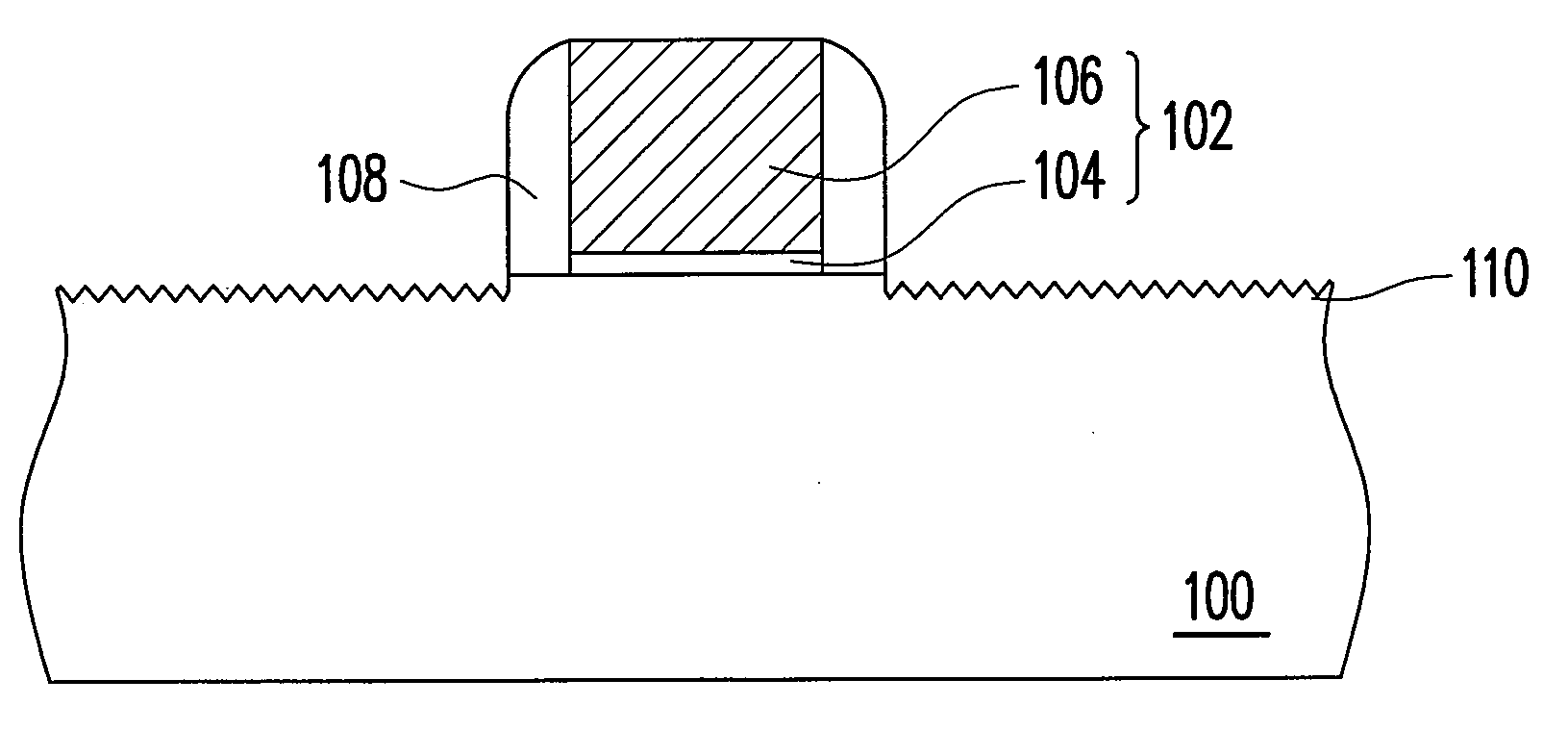
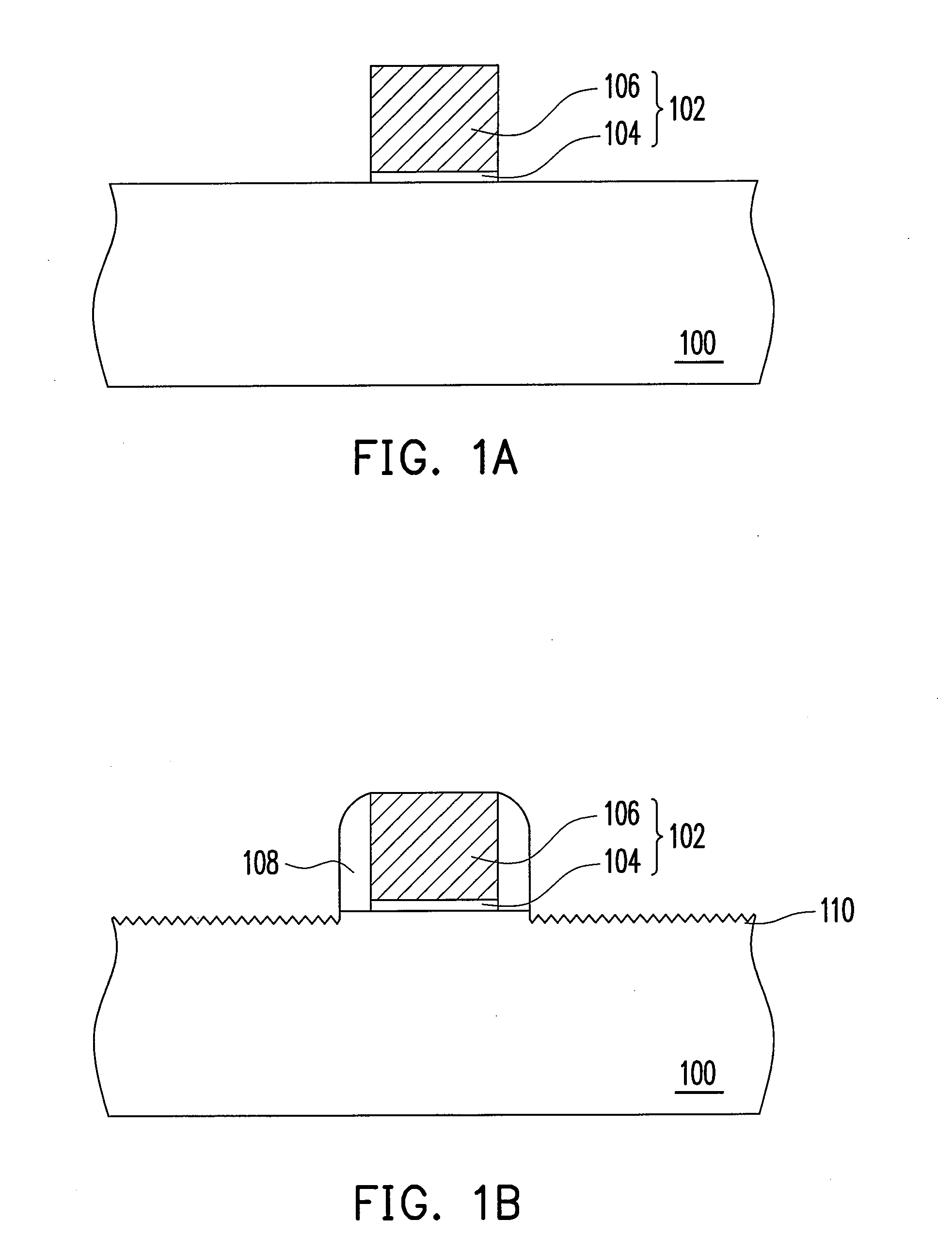
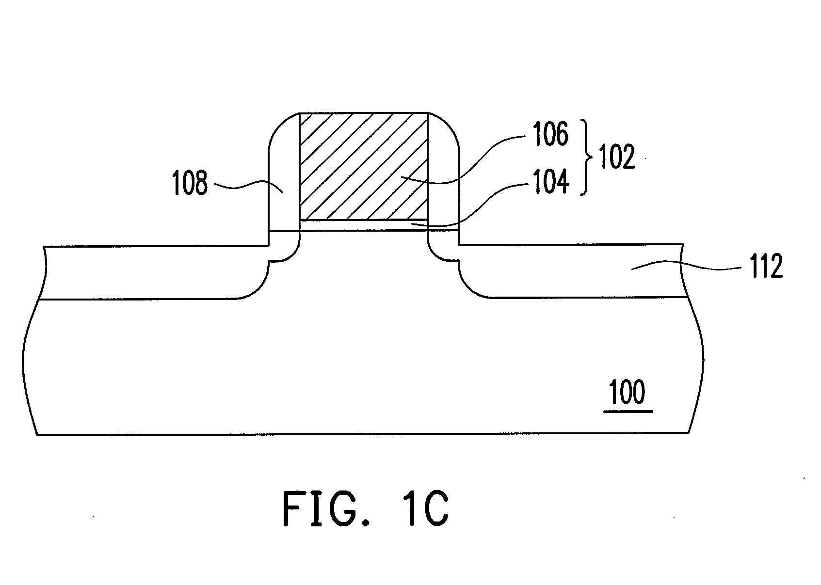
[0035]FIGS. 1A-1C are schematic sectional views of the manufacturing flow of a transistor device according to an embodiment of the present invention.

[0036]Referring to FIG. 1A, a substrate 100 is provided, which is, for example, silicon substrate or other suitable semiconductor materials. Then, a gate structure 102 is formed on the substrate 100. The gate structure 102 is composed of a gate dielectric layer 104 and a gate conductive layer 106. In an embodiment, the material of the gate dielectric layer 104 is silicon oxide or silicon nitride and the gate conductive layer 106 is, for example, composed of a polysilicon layer and a metal silicide layer. The gate structure 102 is formed by the following steps. First, an oxide material layer (not shown) is formed on the substrate 100 by, for example, thermal oxidation. Then, a polysilicon material layer (not shown) and a metal silicide material layer (not shown) are successively formed on the oxide material layer. Afterwards, a lithograp...


PUM

PropertyMeasurementUnit
poweraaaaaaaaaa
poweraaaaaaaaaa
pressureaaaaaaaaaa

Abstract

A method for in-situ repairing plasma damage, suitable for a substrate, is provided. A component is formed on the substrate. The formation steps of the component include a main etching process containing plasma. The method involves performing a soft plasma etching process in the apparatus of the main etching process containing plasma to remove a portion of the substrate. The soft plasma etching process is less than 30% of the power used in the main etching process.

Description

BACKGROUND OF THE INVENTION[0001]1. Field of the Invention[0002]The present invention relates to a method for fabricating transistor device. More particularly, the present invention relates to a method for in-situ repairing plasma damage on substrate.[0003]2. Description of Related Art[0004]With the rapid development of IC industry, the integration of devices is increasingly enhanced. Under such trend, it has been a key issue of study in this field how to avoid short channel effect caused by device miniaturization and how to solve problems such as current leakage and short circuit caused by disposing devices adjacent to each other.[0005]Generally, in order to isolate the gates of adjacent transistors, spacers are disposed at both sides of the gates. Moreover, the spacers can also be used as heavy doping masks to form a source / drain of a transistor. In the current fabrication progress, the spacer has become an essential component of each transistor.[0006]A common method of forming a ...

Claims


Application Information

Patent Timeline
Patent Type & Authority Applications(United States)
IPC IPC(8): H01L21/336
CPCH01L21/0206H01L21/3065H01L29/6659H01L29/66636H01L29/7834
Inventor SU, HSIN-FANGTSAI, SHIH-CHANGLEE, CHUN-HUNG
Owner MACRONIX INT CO LTD
Why Eureka
Try Eureka