
Polishing apparatus

Active Publication Date: 2008-11-20
EBARA CORP
View PDF11 Cites 28 Cited by
  • Summary
  • Abstract
  • Description
  • Claims
  • Application Information

AI Technical Summary

Benefits of technology

[0016]It is therefore an object of the present invention to provide a polishing apparatus which minimizes a process of bringing a top ring into contact with a polishing surface in order to detect the vertical position of the top ring or the vertical position of the polishing surface prior to a polishing process, for thereby increasing a throughput, and which is capable of keeping the top ring in an optimum position at the time of polishing even if a top ring shaft that holds the top ring is extended due to a temperature rise, while dealing with a change in the top ring shaft due to a temperature rise during polishing.
[0017]Another object of the present invention is to provide a polishing apparatus which can prevent a top ring shaft holding a top ring from increasing its temperature even if the polishing apparatus is in continuous operation.
[0018]Still another object of the present invention is to provide a polishing apparatus which keeps a polishing profile constant even if the resiliency (elasticity) of a polishing pad varies due to wear of the polishing pad.

Problems solved by technology

Multilayer interconnections in smaller circuits result in greater steps which reflect surface irregularities on lower interconnection layers.
An increase in the number of interconnection layers makes film coating performance (step coverage) poor over stepped configurations of thin films.
In such polishing apparatus, if the relative pressing force applied between the semiconductor wafer, being polished, and the polishing surface of the polishing pad is not uniform over the entire surface of the semiconductor wafer, then the surface of the semiconductor wafer is polished insufficiently or excessively in different regions thereof depending on the pressing force applied thereto.
The time required to bring the polishing head into contact with the polishing pad and then lift the polishing head increases the overall polishing time of the polishing process, resulting in lowering the throughput of the polishing apparatus.
At this time, since a force of about 1500 N at maximum is applied to a local area of the semiconductor wafer, devices fabricated on the semiconductor wafer may possibly be damaged or broken.
Therefore, the gears, the ball screw, and other mechanical parts tend to cause a large mechanical loss.
When the top ring shaft is actuated for precision feeding, a certain torque limit is imposed on the motor.
However, if the motor is operated at a low torque to feed the top ring shaft, then the motor may stall due to an instantaneous large mechanical loss.
Thus, devices fabricated on the semiconductor wafer are likely to be broken by this load.
However, it needs extra work to install the dummy wafer on the polishing head or the top ring and de-install the dummy wafer from the polishing head or the top ring, and the extra work is responsible for reducing the throughput.

Method used


Image

  • Polishing apparatus
  • Polishing apparatus
  • Polishing apparatus

Examples


Embodiment Construction

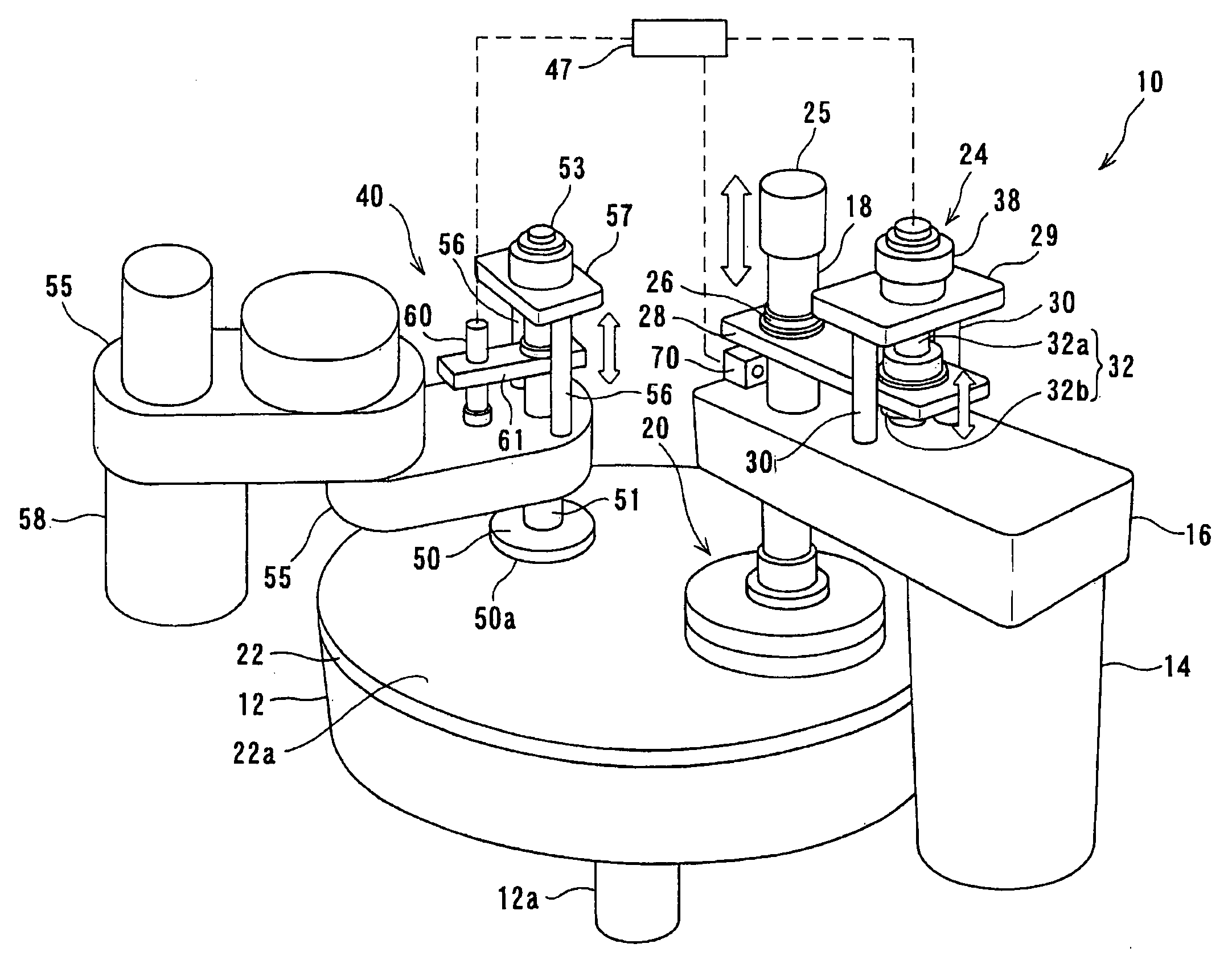
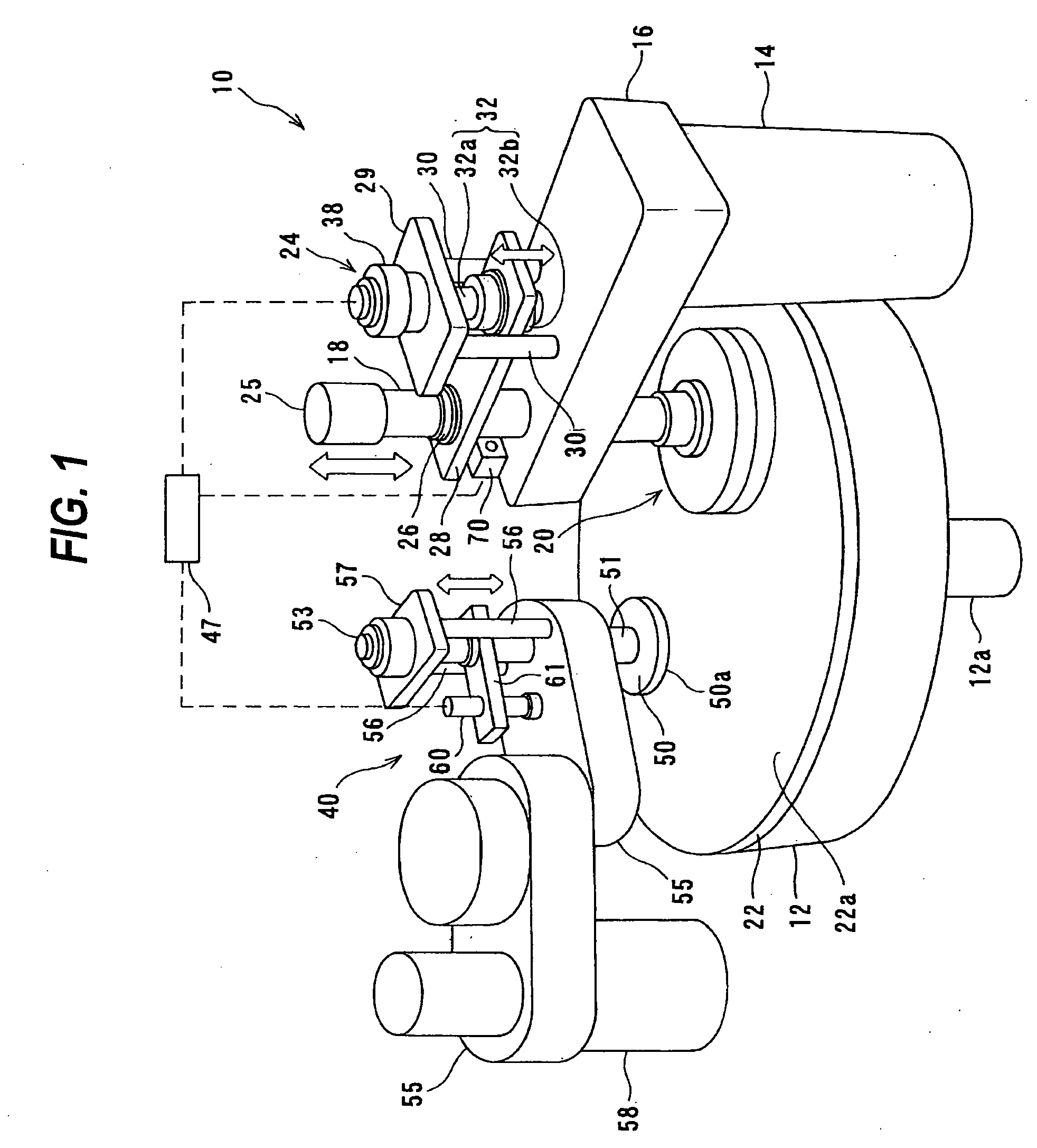
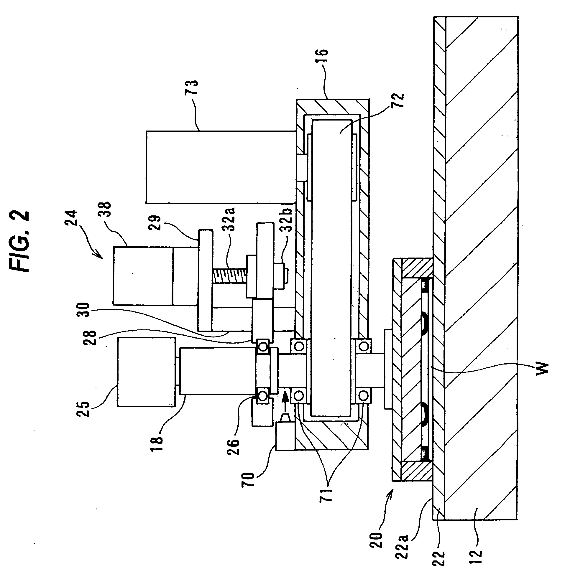
[0080]A polishing apparatus according to embodiments of the present invention will be described below with reference to FIGS. 1 through 18. Like or corresponding parts are denoted by like or corresponding reference numerals throughout drawings and will not be described below repetitively.

[0081]FIG. 1 is a schematic view showing a polishing apparatus 10 according to a first embodiment of the present invention. As shown in FIG. 1, the polishing apparatus 10 has a polishing table 12, a top ring head 16 connected to an upper end of a support shaft 14, a top ring shaft 18 mounted at a free end of the top ring head 16, and a top ring 20 coupled to a lower end of the top ring shaft 18. In the illustrated example, the top ring 20 is substantially in the form of a circular plate. The top ring shaft 18 is coupled to a top ring rotating motor through a coupling device such as a timing belt, and thus the top ring shaft 18 is rotatable. However, in FIG. 1, the top ring rotating motor, the timing...


PUM


Abstract

A polishing apparatus is used for polishing a substrate such as a semiconductor wafer to a flat mirror finish. The polishing apparatus includes a polishing table having a polishing surface, a top ring configured to hold and press the substrate against the polishing surface, a top ring shaft configured to lift and lower the top ring, and an elongation detecting device configured to detect an elongation of the top ring shaft. The polishing apparatus further includes a controller configured to set a vertical position of the top ring at the time of polishing, and control a lifting and lowering mechanism to lower the top ring to a preset polishing position as the set vertical position. The controller corrects the preset polishing position based on the elongation of the top ring shaft which has been detected by the elongation detecting device.

Description

BACKGROUND OF THE INVENTION[0001]1. Field of the Invention[0002]The present invention relates to a polishing apparatus, and more particularly to a polishing apparatus for polishing an object to be polished (substrate) such as a semiconductor wafer to a flat mirror finish.[0003]2. Description of the Related Art[0004]In recent years, high integration and high density in semiconductor device demands smaller and smaller wiring patterns or interconnections and also more and more interconnection layers. Multilayer interconnections in smaller circuits result in greater steps which reflect surface irregularities on lower interconnection layers. An increase in the number of interconnection layers makes film coating performance (step coverage) poor over stepped configurations of thin films. Therefore, better multilayer interconnections need to have the improved step coverage and proper surface planarization. Further, since the depth of focus of a photolithographic optical system is smaller wi...

Claims


Application Information

Patent Timeline
IPC IPC(8): B24B29/00B24B37/07B24B37/10B24B49/10B24B53/02
CPCB24B49/14B24B53/017B24B49/18H01L21/304
Inventor SAITO, KENICHIRONABEYA, OSAMUNAGATA, KIMIHIDETOGAWA, TETSUJI
Owner EBARA CORP
Learn More