Semiconductor light emitting apparatus

a technology of semiconductors and light emitting devices, applied in semiconductor devices, light emitting devices, solid-state devices, etc., can solve the problems of light emitting apparatuses that are difficult to reduce the size of light sources, and the luminous flux decreases, so as to reduce luminance and chromaticity variations

Active Publication Date: 2008-11-27
STANLEY ELECTRIC CO LTD
View PDF6 Cites 110 Cited by
  • Summary
  • Abstract
  • Description
  • Claims
  • Application Information

AI Technical Summary

Benefits of technology

[0014]The presently disclosed subject matter was devised in view of these and other problems and in association with the conventional art. According to an aspect of the presently disclosed subject matter, a light emitting apparatus which includes LED chips can be provided directly with a wavelength conversion layer which reduces variations in chromaticity and luminance.
[0022]The wavelength conversion layer is formed to link between the upper surface portions (substantial light emitting portions) of the plurality of LED chips that are separately provided, thereby allowing emitted light to be provided with reduced variations in luminance and chromaticity within the emission plane.

Problems solved by technology

Nevertheless, this is not enough to eliminate those variations in chromaticity and luminance, but possibly raises another problem in that the light diffusion layer causes a decrease in luminous flux.
However, this type of light emitting apparatus is difficult to reduce its light source in size.

Method used


Image

  • Semiconductor light emitting apparatus
  • Semiconductor light emitting apparatus
  • Semiconductor light emitting apparatus

Examples


first example

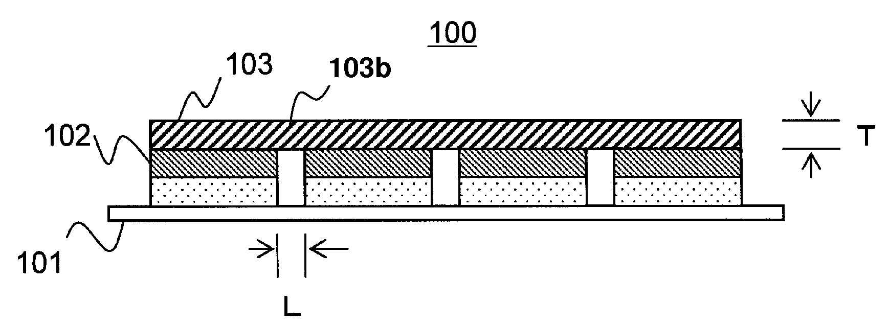
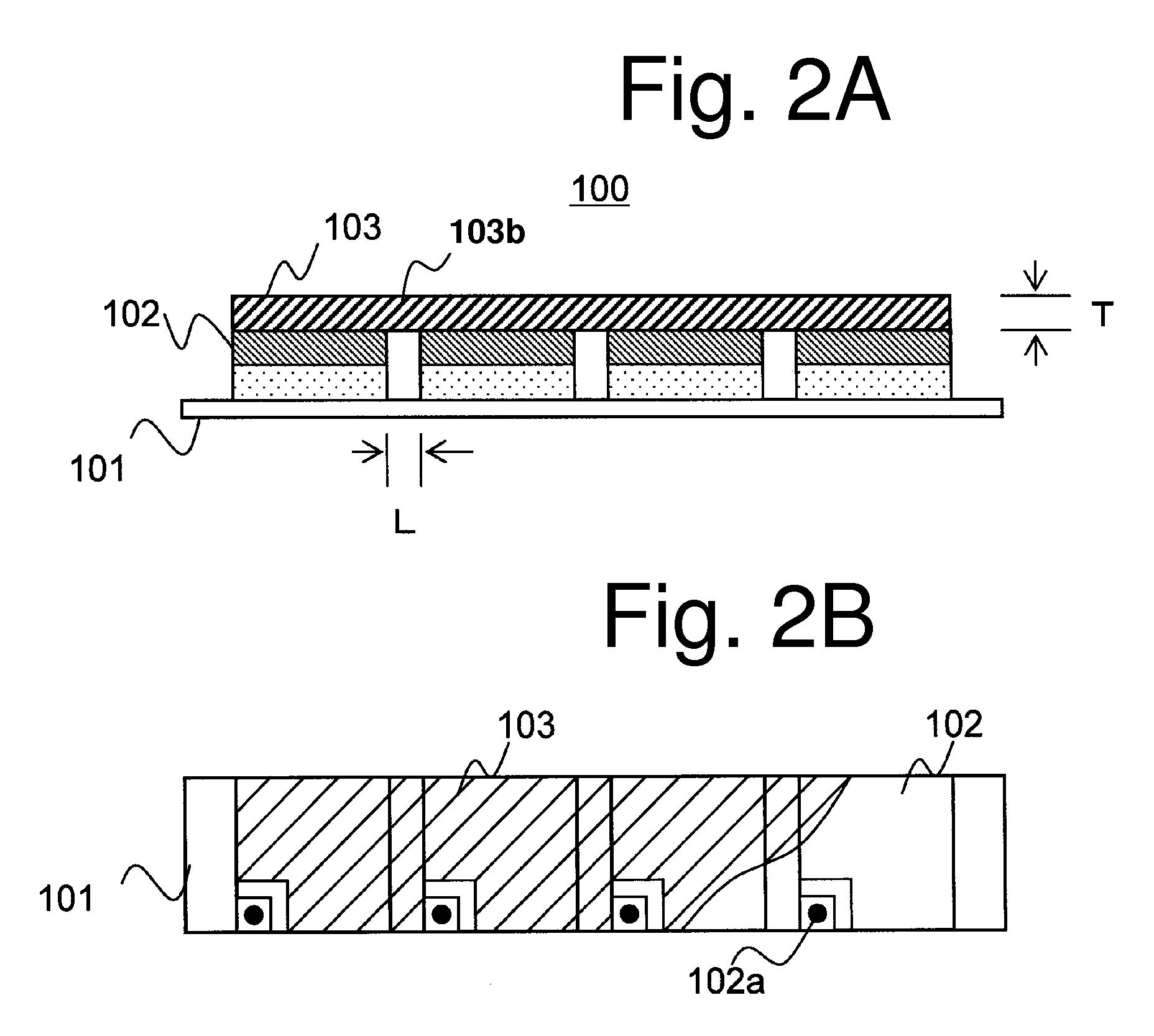
[0074]Four LED chips, each having a side length of 980 μm, were mounted onto a ceramic package (substrate) at a spacing of L=200 μm between the chips. A phosphor layer 200 μm in thickness was formed on the LED chips by stencil printing (metal mask printing).

[0075]To form the phosphor layer, a phosphor dispersion of a silicone-based thermosetting resin was used, which was prepared by mixing the silicone-based thermosetting resin with a 27 wt % YAG-based phosphor and a 13 wt % fumed silica for controlling viscosity. The phosphor layer was printed using a stainless-steel stencil (metal mask) 200 μm in thickness. After having been printed, the phosphor layer was heated at 150 degrees centigrade for two hours to cure the silicone resin, thereby forming the phosphor layer to be substantially the same thickness as the metal mask. After that, the pad sections on the upper surface of the LED chips were bonded with gold wire, thereby fabricating an LED apparatus in the configuration as shown ...

second example

[0082]Four LED chips, each having a side length of 980 μm and a height of 100 μm, were mounted onto a ceramic package (substrate) at a spacing of L=100 μm between the chips using an electrically conductive adhesive made of AuSn and approximately 30 μm in thickness. A one-component thermosetting adhesive liquid silicone resin (white) that contains 30 to 40% of titanium oxide was injected into the three gaps between the chips to fill in the gaps, and then cured by heating to thereby fill the space in between the chips. The silicone resin mixed with titanium oxide has a height of approximately 120 μm, and is lower than the upper surface of the chips that are mounted on the substrate via the electrically conductive adhesive. As in the first example, a phosphor layer of 200 μm in thickness was formed on the LED chips by stencil printing (metal mask printing). Subsequently, the pad sections on the upper surface of the LED chips were bonded with gold wire, thereby fabricating the LED appar...

third example

[0085]Four LED chips, each having a side length of 980 μm and a height of 100 μm, were mounted onto a ceramic package (substrate) at a spacing of L=100 μm between the chips using an electrically conductive adhesive made of AuSn and approximately 30 μm in thickness.

[0086]A dispersed silicone resin mixed with 23 wt % of titanium oxide of an average particle diameter D50 of 21 nm (before dispersed) and 9 wt % of a thickener of fumed silica was printed using a metal mask. The resin was then cured by heating, thereby forming a rib of a height of 200 μm between the chips. Subsequently, a phosphor layer was formed by metal mask printing on the upper surface of the LED chips and on the rib, so that the phosphor layer had a flat top, and a thickness of 200 μm from the upper surface of the chips and of approximately 130 μm from the upper surface of the rib. Subsequently, the pad sections on the upper surface of the LED chips were bonded with gold wire, thereby fabricating the LED apparatus co...


PUM


Abstract

A light emitting apparatus with a combination of a plurality of LED chips and a phosphor layer is provided and can be configured to significantly reduce variations in chromaticity and luminance. The plurality of semiconductor light emitting devices (LED chips) are disposed with a gap therebetween, and the phosphor layer is formed on the upper surface thereof to bridge over the gaps between the LED chips. The phosphor layer may be uniform in thickness, but can be less in thickness over the gaps between the LED chips than on the upper surface of the LED chips. The phosphor layer can be continuously formed on the upper surface of the array of the chips with no phosphor layer present in between the chips. This configuration allows for reducing variations in luminance and chromaticity which may result from the gaps or the phosphor layer present in between the gaps.

Description

[0001]This application claims the priority benefit under 35 U.S.C. § 119 of Japanese Patent Application No. 2007-138213 filed on May 24, 2007, which is hereby incorporated in its entirety by reference.BACKGROUND[0002]1. Technical Field[0003]The presently disclosed subject matter relates to a semiconductor light emitting apparatus which includes an array of a plurality of semiconductor light emitting devices. In particular, the presently disclosed subject matter relates to a semiconductor light emitting apparatus which employs color-converted semiconductor devices to produce a color mixture of primary light emitted by the semiconductor devices and secondary light which includes light that has been color-converted by a color-converting phosphor material or the like using the primary light as excitation light.[0004]2. Description of the Related Art[0005]Semiconductor light emitting apparatuses which employ semiconductor light emitting devices (hereinafter referred to as “LED chips” or ...

Claims


Application Information

Patent Timeline
Patent Type & Authority Applications(United States)
IPC IPC(8): H01L33/00H01L33/50H01L33/56H01L33/62
CPCF21K9/00H01L25/0753H01L33/505H01L27/15H01L2924/0002H01L33/50H01L2924/00
Inventor AJIKI, SHUICHIKAWAKAMI, YASUYUKIAKAGI, TSUTOMUHARADA, MITSUNORI
Owner STANLEY ELECTRIC CO LTD
Why Eureka
Try Eureka