Leadframe package

a leadframe and package technology, applied in the field of leadframes, can solve the problems of increasing the cost of packaging each die accordingly, and increasing the number of external connection pins of the leadframe package, so as to achieve less noise interference and improve the quality of electronic signals

Active Publication Date: 2008-11-27
MEDIATEK INC
View PDF24 Cites 51 Cited by
  • Summary
  • Abstract
  • Description
  • Claims
  • Application Information

AI Technical Summary

Benefits of technology

[0015]With these embodiments, e.g. improved leadframe and its manufacturing process, semiconductor pac...

Problems solved by technology

The functionality of the integrated circuit chips is becoming more and more complicated, leading to increased number of external connection pins of the leadframe package.
As the pin count is increased, the cost of packaging each die is increased accordingly.
However, narrowing the lead pitch results in increase in the level of mutual inductance and mutual capacitance generated from the leads of the package.
Thus, leadframe packages are typically considered to be unsuitable for high-speed semiconductor dies, which transmit signals at high speeds, since the relatively high inductance and c...

Method used


Image

  • Leadframe package
  • Leadframe package
  • Leadframe package

Examples


Embodiment Construction

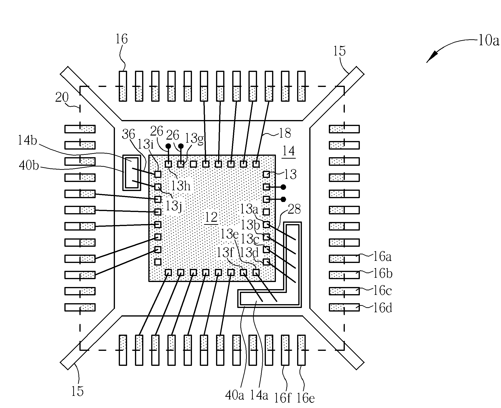
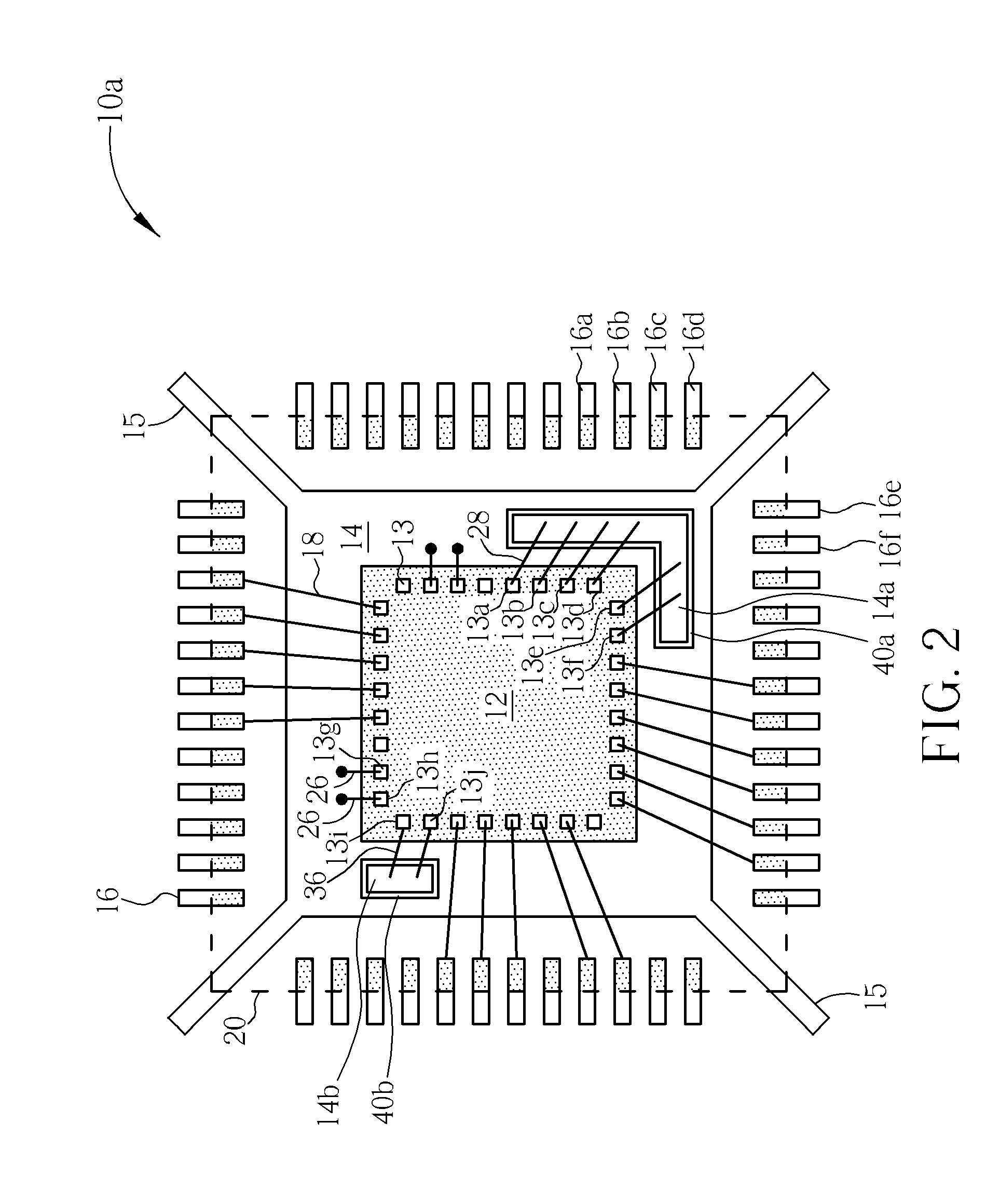
[0035]The improved leadframe package structure, as described below, is suited for the applications including, but not limited to, LQFP (Low-Profile Quad Flat Pack) packaging, TQFP (Thin Quad Flat Pack) packaging, QFN (Quad Flat Non-leaded) packaging, DFN (Dual Flat No-lead) packaging, multi-zone QFN, and multi-die flip-chip packaging.

[0036]The present invention is capable of pushing the limits of conventional leadframe package by sparing or releasing a number of the leads that used to be wire bonded to ground pads, power pads or some signal pads on a packaged semiconductor die. Besides, the present invention is capable of improving electrical performance of the integrated circuit package by utilizing separate grounding systems on the die pad.

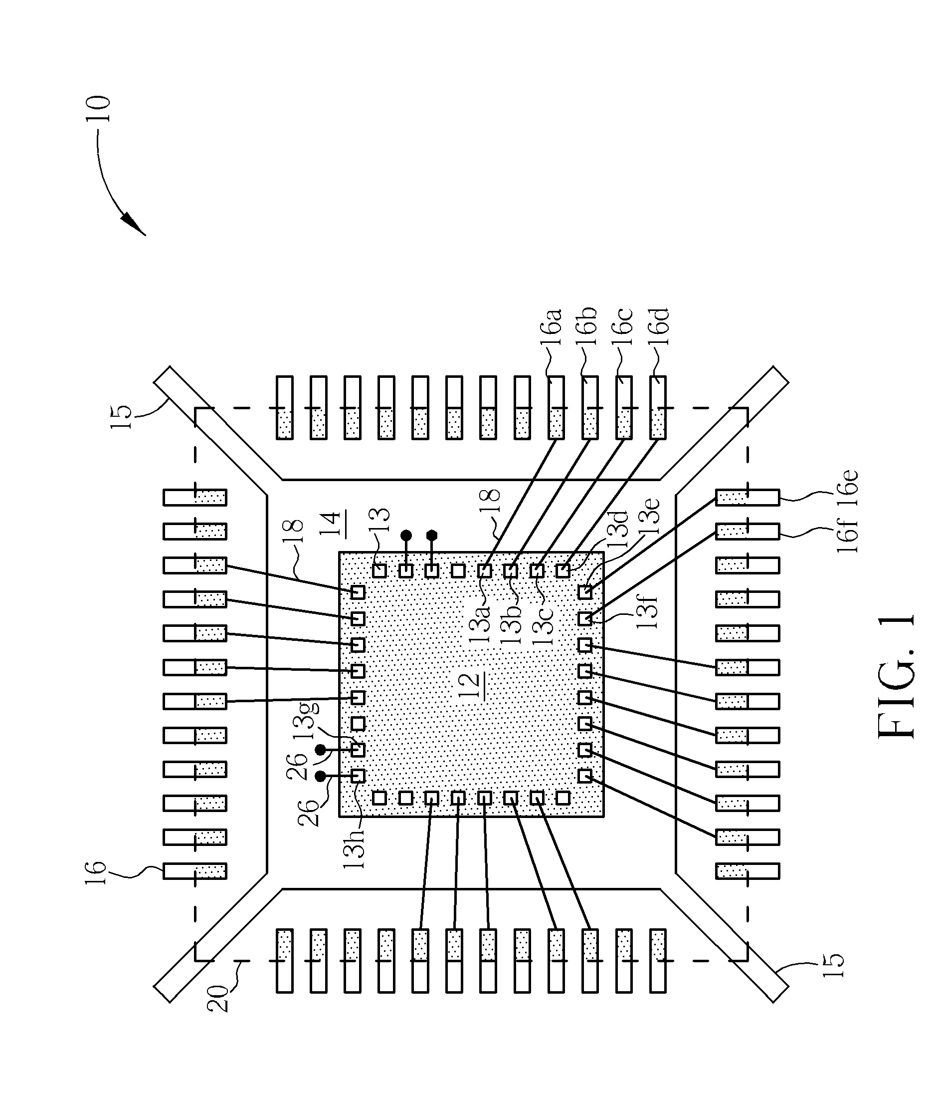
[0037]FIG. 1 illustrates a perspective top view of a leadframe package 10. As shown in FIG. 1, the leadframe package 10 includes a semiconductor die 12, an example of a semiconductor device that is mounted on a die pad 14. A plurality of bond pa...


PUM


Abstract

A leadframe package includes a die pad with four unitary, outwardly extending slender bars; a plurality of leads arranged along periphery of the die pad; a separate pad segment separated from the die pad and isolated from the plurality of leads; a semiconductor die mounted on an upper side of the die pad, wherein the semiconductor die contains first bond pads wire-bonded to respective the plurality of leads and a second bond pad wire-bonded to the separate pad segment; and a molding compound encapsulating the semiconductor die, the upper side of the die pad, the first suspended pad segment and inner portions of the plurality of leads.

Description

CROSS REFERENCE TO RELATED APPLICATIONS[0001]This application is a continuation-in-part of U.S. application Ser. No. 11 / 964,054 filed Dec. 26, 2007. This application also claims the benefit of U.S. provisional application No. 60 / 871,993 filed Dec. 27, 2006.BACKGROUND OF THE INVENTION[0002]1. Field of the Invention[0003]The present invention relates to a leadframe used for semiconductor devices and more particularly, to a leadframe package with multiple exposed pads and method for fabricating the same.[0004]2. Description of the Prior Art[0005]Semiconductor dies are conventionally enclosed in plastic packages that provide protection from hostile environments and enable electrical interconnection between the semiconductor die and a substrate such as a printed circuit board (PCB). Such an integrated circuit (IC) package includes a metal leadframe, a semiconductor die mounted on a unitary die pad of the leadframe, and bond wires electrically connecting bond pads on the semiconductor die...

Claims


Application Information

Patent Timeline
IPC IPC(8): H01L23/495
CPCH01L21/4828H01L21/4832H01L23/3107H01L23/49503H01L23/49531H01L23/49541H01L23/49548H01L23/49575H01L24/05H01L24/06H01L24/49H01L2224/0401H01L2224/05639H01L2224/05644H01L2224/05664H01L2224/05669H01L2224/16H01L2224/48091H01L2224/48137H01L2224/48247H01L2224/48257H01L2224/4912H01L2224/49171H01L2224/49175H01L2224/73265H01L2924/01028H01L2924/01029H01L2924/01046H01L2924/01047H01L2924/0105H01L2924/01075H01L2924/01077H01L2924/01078H01L2924/01079H01L2924/01082H01L2924/014H01L2924/14H01L2924/18301H01L2924/19042H01L2924/19107H01L2924/30105H01L2924/30107H01L24/48H01L2224/32245H01L2924/01033H01L2924/01044H01L2924/01076H01L2224/16245H01L2224/05554H01L2224/04042H01L2924/00014H01L2924/00H01L2924/00012H01L2924/181H01L24/14H01L2224/49109H01L24/73H01L2224/45099
Inventor CHEN, NAN-JANGLIN, HONG-CHIN
Owner MEDIATEK INC
Why Eureka
Try Eureka