Front panel for plasma display panel and method for producing the same, and plasma display panel

a plasma display panel and plasma display technology, which is applied in the manufacture of electrode systems, cold cathode manufacturing, and electric discharge tubes/lamps, etc., can solve the problems of poor apt, and reduced pdp production yield, so as to reduce the incidence of chipping, enhance the stability of initial electron emission, and reduce the effect of voltag

Inactive Publication Date: 2008-11-27
PANASONIC CORP
View PDF1 Cites 23 Cited by
  • Summary
  • Abstract
  • Description
  • Claims
  • Application Information

AI Technical Summary

Benefits of technology

[0050]In the front panel for a plasma display panel of the present invention, the annealed layer is formed on at least the exposed surface of each of the powder components, which does not contact the dielectric-protection layer. Thereby, it is possible to provide a front panel for a plasma display panel which can suppress the incidence of chipping of the barrier rib of the rear panel for a plasma display panel, can enhance the stability of initial electron emission in the dielectric layer, and can reduce a voltage required for maintaining a wall charge.
[0051]In accordance with the method for producing a front panel for a plasma display panel of the present invention, after the powder components are dispersed on the dielectric-protection layer, an energy wave is irradiated to the exposed surface of each of the powder components to form the annealed layer. Thereby, it is possible to provide a method for producing a front panel for a plasma display panel which can suppress the i

Problems solved by technology

Therefore, the barrier rib becomes apt to chip and there is an issue that the production yield of the PDP is reduced.
However, in the case where the average particle diameter of the powder components is set at about 2.0 μm, there are

Method used


Image

  • Front panel for plasma display panel and method for producing the same, and plasma display panel
  • Front panel for plasma display panel and method for producing the same, and plasma display panel
  • Front panel for plasma display panel and method for producing the same, and plasma display panel

Examples


first embodiment

[0068]A constitution of a PDP of a first embodiment of the present invention will be described referring to FIGS. 1 to 3.

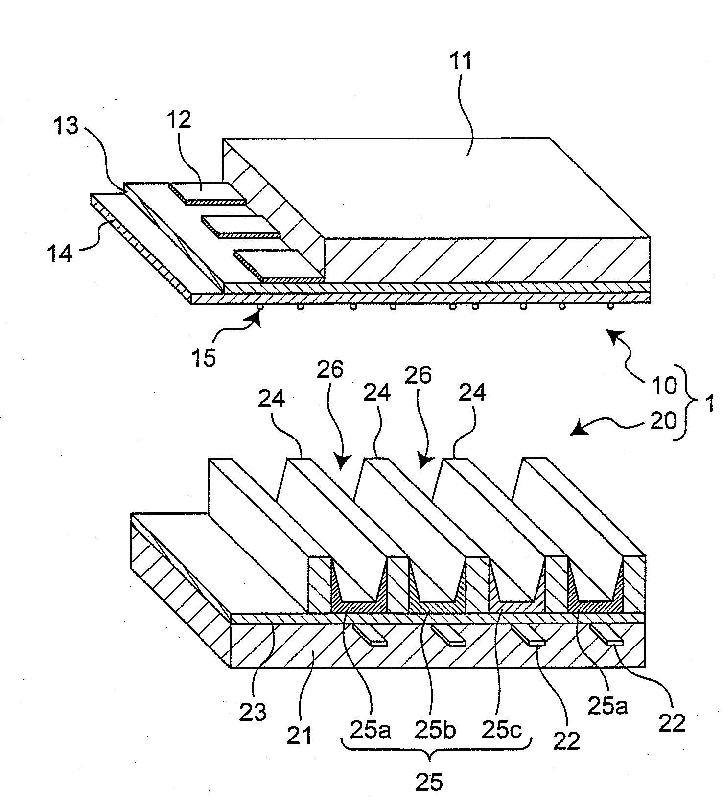
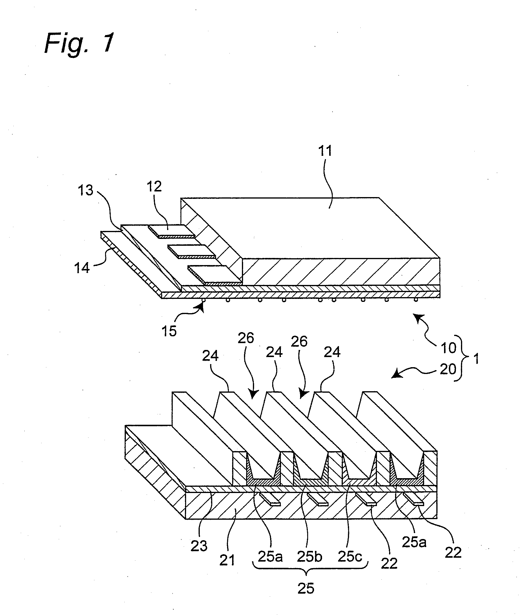
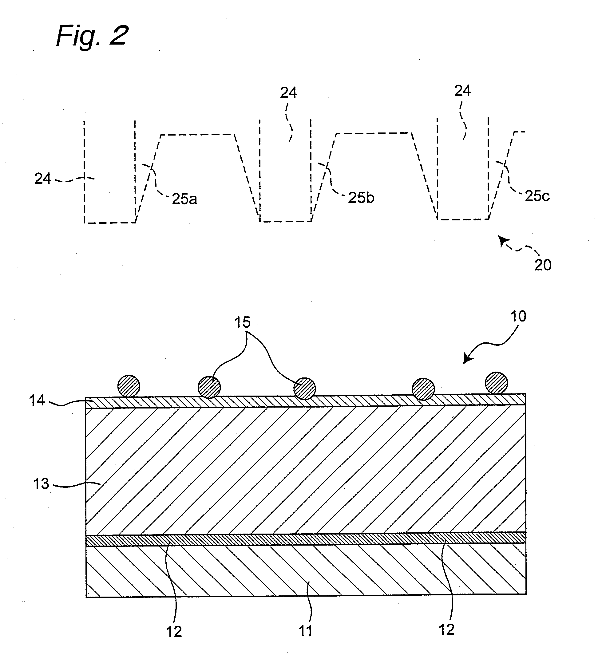
[0069]FIG. 1 is a perspective view schematically showing a basic constitution of a PDP 1 according to the first embodiment of the present invention. Further, in FIG. 1, a front panel 10 and a rear panel (back panel) 20 of the PDP 1 are illustrated away from each other for ease of reference. FIG. 2 is a partially enlarged sectional view of the front panel 10. In FIG. 2, the arrangement of the front panel 10 is vertically opposite in direction to that of the front panel 10 in FIG. 1. FIG. 3 is a partially enlarged sectional view of FIG. 2.

[0070]In FIG. 1, the PDP 1 includes a front panel 10 for a PDP (hereinafter, referred to as a front panel) and a rear panel 20 for a PDP (hereinafter, referred to as a rear panel) opposed to the front panel 10. A sealing member (not shown) such as glass frit is located on the periphery of a space between the front panel 10 and the ...

second embodiment

[0116]A front panel for a PDP of a second embodiment of the present invention will be described referring to FIGS. 8 to 10. FIG. 8 is a flow chart showing a method for producing a PDP according to the second embodiment of the present invention. FIG. 9 is a view schematically showing the state of forming an annealed layer on an entire surface of each of powder components of the PDP according to the second embodiment of the present invention. FIG. 10 is a partially enlarged sectional view showing a constitution of the powder component of the PDP according to the second embodiment of the present invention.

[0117]In the foregoing method of producing the front panel for a PDP of the first embodiment, after the powder components 15 are formed on the dielectric-protection layer 14 (step S7), the annealed layer 15a is formed on the exposed surface of each of the powder components 15 (step S8). In the method for producing a front panel for a PDP according to the second embodiment of the prese...


PUM


Abstract

The present invention provides a front panel for a plasma display panel which can suppress the incidence of chipping of the barrier rib of a rear panel for a PDP, can enhance the stability of initial electron emission in a dielectric layer, and can reduce a voltage required for maintaining a wall charge. The front panel for a plasma display panel includes a substrate, a plurality of electrodes formed on the substrate, a dielectric layer formed to cover the respective electrodes and the substrate, a dielectric-protection layer formed to cover the dielectric layer, and powder components dispersed on the dielectric-protection layer, wherein an annealed layer having a thickness of 10 to 300 nm is formed on at least the exposed surface of each of the powder components, wherein said exposed surface does not contact the dielectric-protection layer.

Description

BACKGROUND OF THE INVENTION[0001]The present invention relates to a front panel for a plasma display panel including powder components and a method for producing the same, and a plasma display panel.[0002]Hitherto, as a display device for displaying high-definition television images in a large screen, expectations for a display device using a plasma display panel (hereinafter, referred to as a PDP) have been heightening. Hereinafter, a constitution of a PDP of a conventional example will be described.[0003]The PDP of a conventional example is provided with a front panel and a rear panel.[0004]The front panel includes a front glass substrate, a plurality of display electrodes formed into stripe form on one surface of the front glass substrate, a dielectric glass layer covering these display electrodes and a dielectric-protection layer covering the dielectric glass layer.[0005]The rear panel includes a rear glass substrate, a plurality of address electrodes formed into stripe form on ...

Claims


Application Information

Patent Timeline
IPC IPC(8): H01J17/49H01J9/02H01J11/22H01J11/24H01J11/34H01J11/36H01J11/38H01J11/40H01J11/42H01J11/50
CPCH01J9/02H01J11/12H01J11/40H01J11/42H01J11/38
Inventor SAITOH, MITSUOMORITA, MASASHIMAESHIMA, SATOSHIYAMASHITA, HIDEKIFUJII, TSUTOMUKAMIKIHARA, NOBUYUKI
Owner PANASONIC CORP
Why Eureka
Try Eureka