Printed circuit board, production method therefor, electronic-component carrier board using printed circuit board, and production method therefor

a technology of electronic components and printed circuit boards, which is applied in the direction of printed circuits, fixed connections, conductive pattern formation, etc., can solve the problems of reducing productivity, reducing the efficiency of flip chip technology, and reducing the time required for wire bonding

Inactive Publication Date: 2008-12-04
MEIKO ELECTRONICS CO LTD
View PDF4 Cites 80 Cited by
  • Summary
  • Abstract
  • Description
  • Claims
  • Application Information

AI Technical Summary

Benefits of technology

[0010]A purpose of the present invention is to provide a printed circuit board, a method of producing the printed circuit board, an electronic-component carrier board using the printed circuit board, and a method of producing the electronic-component carrier board, that allow the flip chip technology to mount electronic components, such as semiconductor devices, on the printed circuit board, with no such problems of a further multi-layered and a larger structure for the printed circuit board, or the electronic-component carrier board using this printed circuit board and also lower productivity.

Problems solved by technology

Wire bonding, however, poses several problems to recent larger scale integration of semiconductor devices with increased number of terminals that connect a printed circuit board and semiconductor devices.
Time required for wire bonding thus becomes longer as the number of such terminal increases, which results in lower productivity.
The flip chip technology also has difficulty in printing bumps in cavities for connection terminals provided in the cavities of a printed circuit board.
Such bumps can be formed with wire bonding, which, however, results in a further multi-layered and a larger structure for the printed circuit board, or the electronic-component carrier board using this printed circuit board and also lower productivity, according to the same reason as discussed above.

Method used


Image

  • Printed circuit board, production method therefor, electronic-component carrier board using printed circuit board, and production method therefor
  • Printed circuit board, production method therefor, electronic-component carrier board using printed circuit board, and production method therefor
  • Printed circuit board, production method therefor, electronic-component carrier board using printed circuit board, and production method therefor

Examples


Embodiment Construction

[0031]Embodiments of a printed circuit board, a method of producing the printed circuit board, an electronic-component carrier board using the printed circuit board, and a method of producing the electronic-component carrier board will be disclosed with reference to the attached drawings.

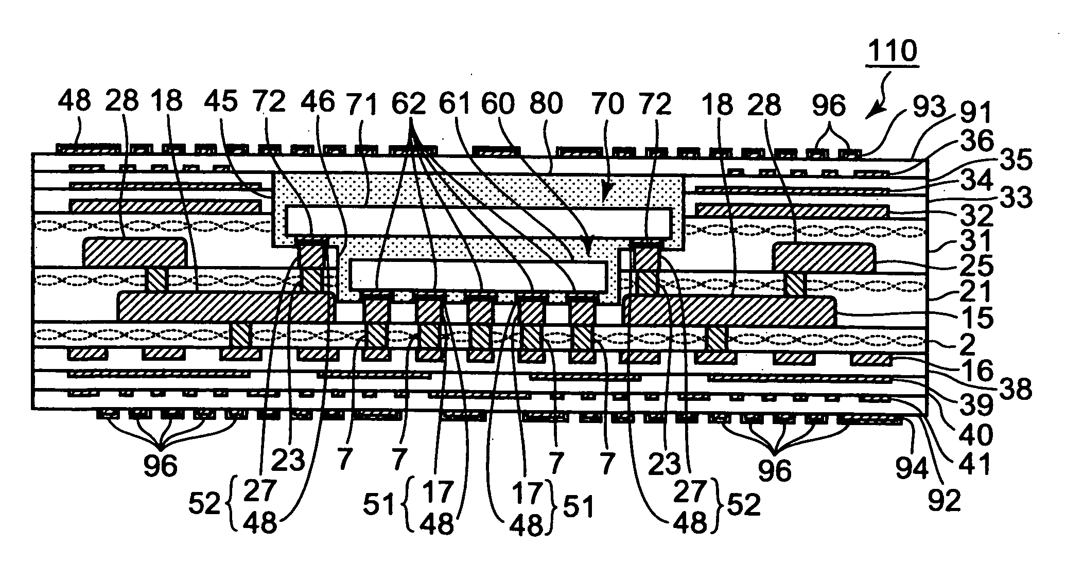
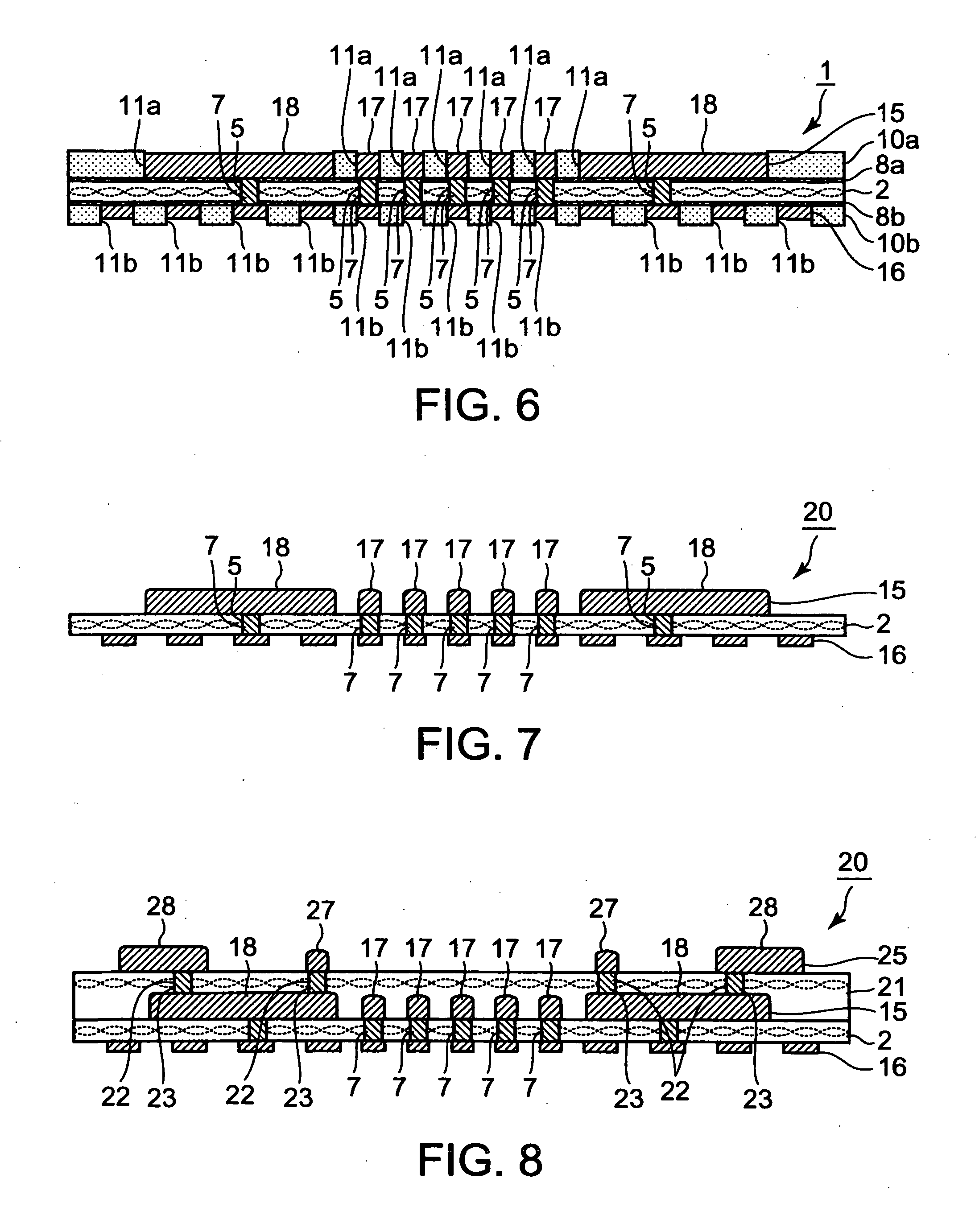
[0032]Disclosed first with reference to FIGS. 1 to 13 are embodiments of a printed circuit board having cavities with electronic components, such as semiconductor devices, housed therein and a method of producing the printed circuit board.

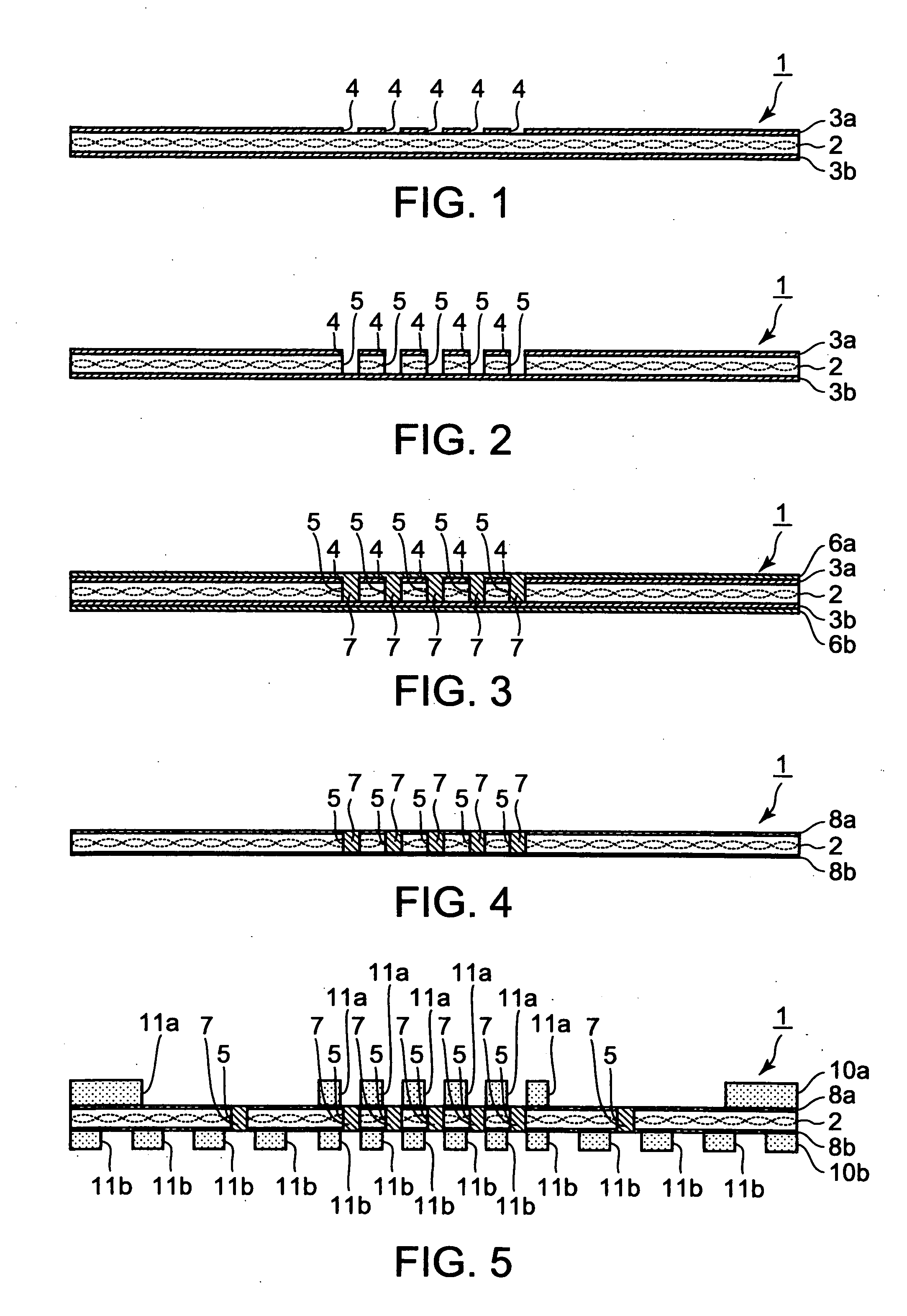
[0033][First Step in FIG. 1]

[0034]Prepared first is a board (or substrate) 1 composed mainly of a core material 2 and copper foils 3a and 3b on both sides. The copper foil 3a is then partially etched to have openings 4 so that the core material 2 is exposed therethrough. The core material 2 is made of a sheet-like reinforcement material (or stiffener), such as glass cloth, impregnated with insulating resin, such as epoxy resin and hardened. The reinforcement materi...


PUM

PropertyMeasurementUnit
thicknessaaaaaaaaaa
entrance diameteraaaaaaaaaa
diameteraaaaaaaaaa

Abstract

A printed wiring board has a substrate having a first surface and a second surface on both sides of the substrate. A cavity is provided on the first surface. The cavity caves in towards the second surface. Several bumps are formed in the cavity as protruding towards the first surface. An insulation layer is filled in the cavity. The bumps are isolated from one another by the insulation layer. The top of each bump that protrudes towards the first surface and a zone in the cavity and close to the top are exposed in the cavity without being covered by the insulation layer.

Description

CROSS-REFERENCE TO RELATED APPLICATIONS[0001]This application is based on and claims the benefit of priority from the prior Japanese Patent Application No. 2007-145198 filed on May 31, 2007, the entire contents of which is incorporated herein by reference.BACKGROUND OF THE INVENTION[0002]The present invention relates to a printed circuit board, a method of producing the printed circuit board, an electronic-component carrier board using the printed circuit board, and a method of producing the electronic-component carrier board. Especially, this invention relates to a printed circuit board having cavities with electronic components, such as semiconductors, housed therein, a method of producing the printed circuit board, an electronic-component carrier board using the printed circuit board, and a method of producing the electronic-component carrier board.[0003]Electronic equipment, such as a personal computer, employs an electronic-component carrier board, such as a semiconductor packa...

Claims


Application Information

Patent Timeline
Patent Type & Authority Applications(United States)
IPC IPC(8): H05K3/10H01R12/06H01R12/51
CPCH01L23/13Y10T29/49155H01L23/49822H01L25/0657H01L2224/16H01L2225/06517H01L2924/01078H01L2924/01079H01L2924/15153H01L2924/1517H05K1/183H05K1/186H05K3/0044H05K3/4652H05K3/4697H05K2201/09481H05K2201/09845H05K2201/10515H05K2203/0228H01L2924/01019H01L2224/16225H01L2924/15151H01L2224/16235H01L23/49816H01L2224/0554H01L2224/05568H01L2224/05573H01L2924/00014H01L2924/15156H01L2224/05599H01L2224/0555H01L2224/0556
Inventor KINOSHITA, TOHRUKANAI, TOSHINOBU
Owner MEIKO ELECTRONICS CO LTD
Why Eureka
Try Eureka