Piezoelectric thin film, piezoelectric material, and fabrication method of piezoelectric thin film and piezoelectric material, and piezoelectric resonator, actuator element, and physical sensor using piezoelectric thin film

a technology which is applied in the field of piezoelectric thin film and piezoelectric material, can solve the problems that the research on improving the piezoelectric response of aluminum nitride is hardly carried out, and achieves the effect of reducing voltage, further increasing the operation range at the same voltage, and improving the piezoelectric respons

Active Publication Date: 2008-12-04
NAT INST OF ADVANCED IND SCI & TECH +1
View PDF3 Cites 61 Cited by
  • Summary
  • Abstract
  • Description
  • Claims
  • Application Information

AI Technical Summary

Benefits of technology

[0016]The inventors of the present invention made a supposition that addition of an appropriate amount of scandium to aluminum nitride can vary a crystal structure of aluminum nitride and improve a piezoelectric response of aluminum nitride. The inventors devoted to research of an amount of scandium to be added and has attained the present invention.
[0052]By setting the temperature of the substrate in the aforesaid range to which substrate aluminum and scandium are adhered, a piezoelectric response of the aluminum nitride thin film that contains scandium can be further improved.

Problems solved by technology

Therefore, a research for improving a piezoelectric response of aluminum nitride is hardly carried out.

Method used


Image

  • Piezoelectric thin film, piezoelectric material, and fabrication method of piezoelectric thin film and piezoelectric material, and piezoelectric resonator, actuator element, and physical sensor using piezoelectric thin film
  • Piezoelectric thin film, piezoelectric material, and fabrication method of piezoelectric thin film and piezoelectric material, and piezoelectric resonator, actuator element, and physical sensor using piezoelectric thin film
  • Piezoelectric thin film, piezoelectric material, and fabrication method of piezoelectric thin film and piezoelectric material, and piezoelectric resonator, actuator element, and physical sensor using piezoelectric thin film

Examples


embodiment 1

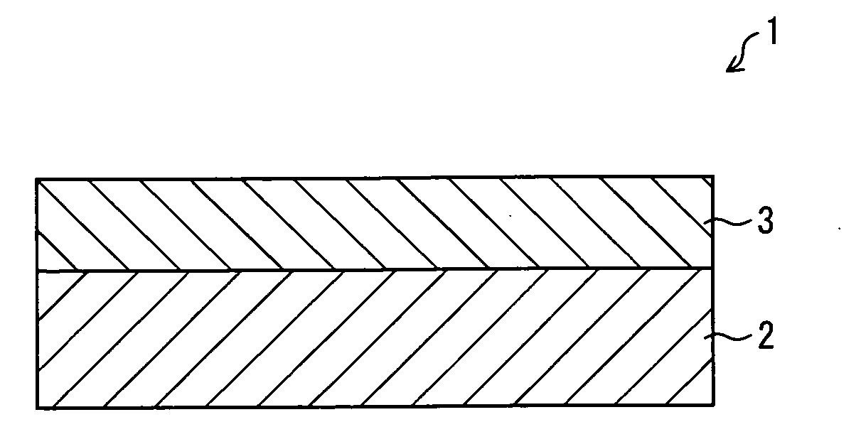
[0068]One embodiment of a piezoelectric thin film of the present invention is explained below as Embodiment 1, with reference to FIGS. 1 and 2.

[0069]Note that a specific application of the piezoelectric thin film of the present invention is not specifically limited in case where the piezoelectric thin film is used in a piezoelectric element that utilizes a piezoelectric phenomenon. For example, the piezoelectric thin film can be applied to an SAW device or an RF-MEMS device. A “piezoelectric material” in the present specification and the like indicates a substance that has a characteristic to produce a potential difference in response to application of mechanical force, that is, a piezoelectric characteristic (hereinafter, also referred to as piezoelectric response). Moreover, a “piezoelectric thin film” indicates a thin film that has the characteristic.

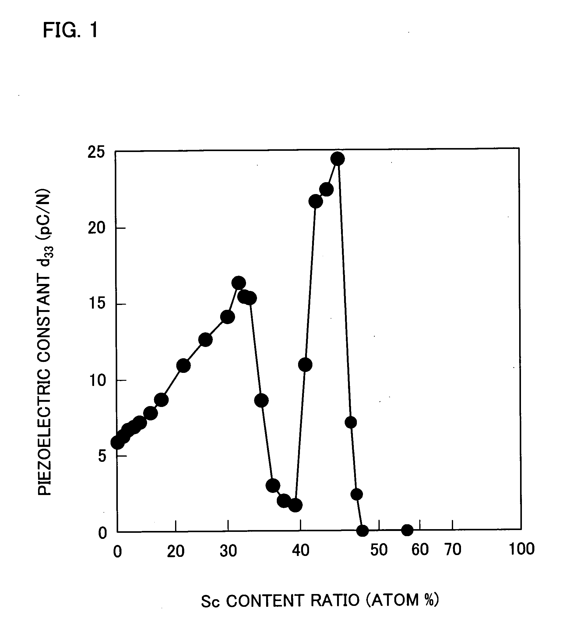
[0070]Further, “atom %” in the present specification and the like indicates atom percentage. More specifically, the “atom %” indica...

embodiment 2

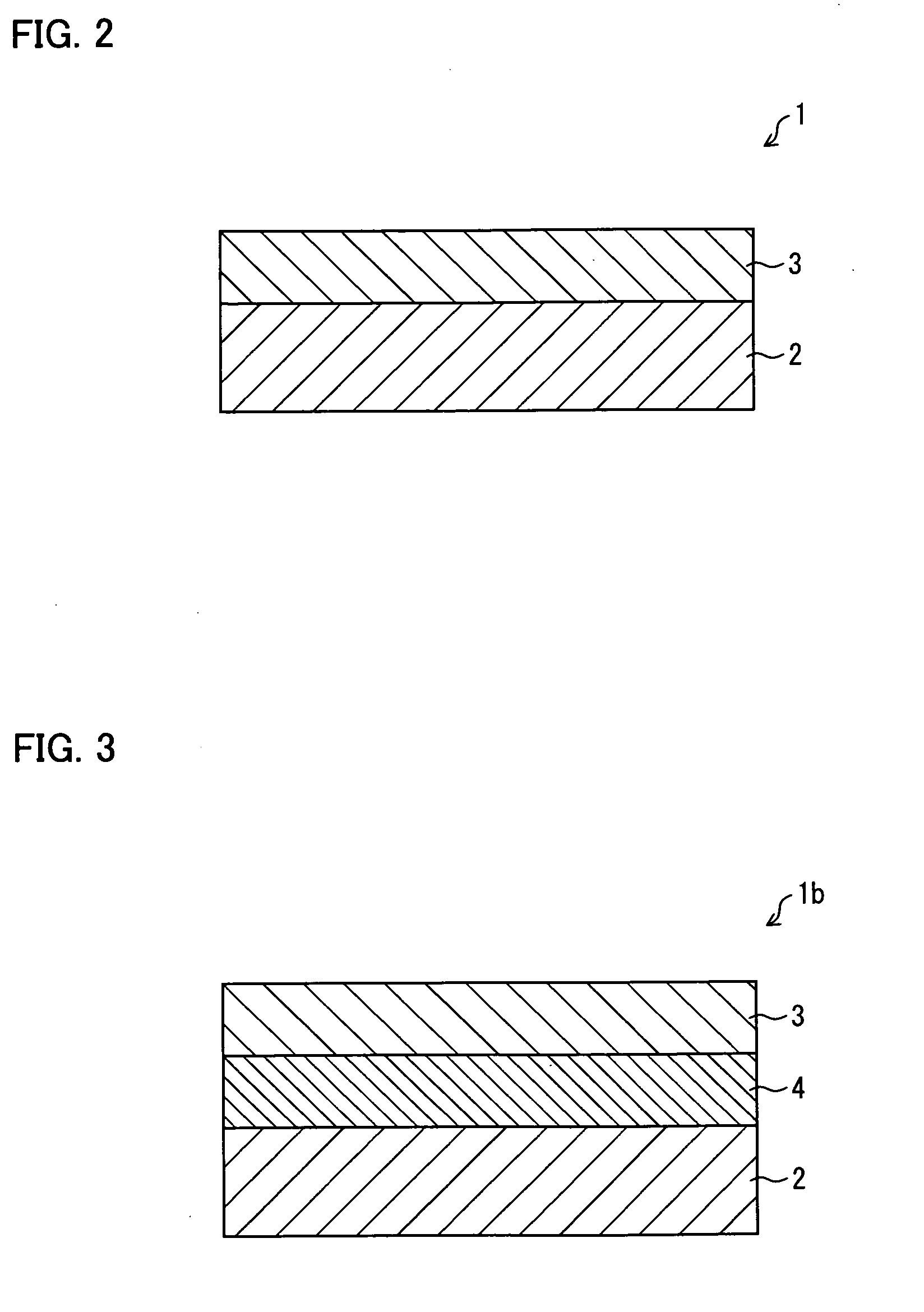
[0086]Another embodiment of a piezoelectric thin film of the present invention is explained below as Embodiment 2, with reference to FIGS. 3 through 5. In the present Embodiment, members given the same reference numerals as in Embodiment 1 respectively have identical functions. Further, the same terms as in Embodiment 1 have identical meanings.

[0087](Structure of Piezoelectric Thin Film 1b)

[0088]As illustrated in FIG. 3, a piezoelectric thin film 1b has an intermediate layer 4 that is formed so as to intervene between a substrate 2 and an Sc-containing aluminum nitride thin film 3. That is, in the piezoelectric thin film 1b, the Sc-containing aluminum nitride thin film 3 is provided on the substrate via the intermediate layer 4. The substrate 2 and the Sc-containing aluminum nitride thin film 3 are explained in Embodiment 1 and detailed explanations thereof are emitted here. Accordingly, in the present embodiment, only the intermediate layer 4 is explained below. FIG. 3 is a cross s...

embodiment 3

[0105]One embodiment of a fabrication method of a piezoelectric thin film 1 of Embodiment 1 is explained below as Embodiment 3, with reference to FIG. 6. Note that application of an Sc-containing aluminum nitride thin film is not specifically limited as long as the Sc-containing aluminum nitride thin film is used in a piezoelectric element that utilizes a piezoelectric phenomenon. For example, a piezoelectric thin film that includes the Sc-containing aluminum nitride thin film can be used in an SAW device or an RF-MEMS device. Moreover, in the present embodiment, the same terms as in Embodiment 1 have identical meanings.

[0106]A fabrication method of the piezoelectric thin film 1 includes a sputtering process in which scandium and aluminum are simultaneously sputtered onto a substrate 2 (for example, a silicon (Si) substrate) in a nitrogen gas (N2) atmosphere or an atmosphere of a mixture of nitrogen gas (N2) and argon gas (Ar). This makes it possible to form an Sc-containing aluminu...


PUM

PropertyMeasurementUnit
temperatureaaaaaaaaaa

Abstract

A piezoelectric thin film of the present invention includes an aluminum nitride thin film that contains scandium. A content ratio of scandium in the aluminum nitride thin film is 0.5 atom % to 50 atom % on the assumption that a total amount of the number of scandium atoms and the number of aluminum atoms is 100 atom %. According to this arrangement, the piezoelectric thin film of the present invention can improve a piezoelectric response while keeping characteristics of elastic wave propagation speed, Q value, and frequency-temperature coefficient that the aluminum nitride thin film has.

Description

[0001]This Nonprovisional application claims priority under 35 U.S.C. § 119(a) on Patent Applications No. 144851 / 20007 filed in Japan on May 31, 2007 and No. 098480 / 2008 filed in Japan on Apr. 4, 2008, the entire contents of which are hereby incorporated by reference.FIELD OF THE INVENTION[0002]The present invention relates to a piezoelectric material and a piezoelectric thin film, in particular, to a piezoelectric material in which scandium is added to aluminum nitride, and a piezoelectric film in which scandium is added to aluminum nitride.BACKGROUND OF THE INVENTION[0003]A device that utilizes a piezoelectric phenomenon is applied in a wide range of fields. The application of such a device is increasing particularly in portable apparatuses such as mobile phones for which size reduction and power consumption saving are strongly demanded. IF (Intermediate Frequency) and RF (Radio Frequency) filters are examples of the application of the device. Specific examples of the IF and RF fi...

Claims


Application Information

Patent Timeline
Patent Type & Authority Applications(United States)
IPC IPC(8): H01L41/187B05D5/12H01L41/316
CPCB81B3/0021B81B2201/0271B81B2201/032H01L41/187H01L41/316H03H9/173H03H9/02015H03H9/02574H01L41/0815H01L41/094H01L41/1136H10N30/10516H10N30/2042H10N30/306H10N30/853H10N30/076
Inventor AKIYAMA, MORITOKAMOHARA, TOSHIHIROUENO, NAOHIROKANO, KAZUHIKOTESHIGAHARA, AKIHIKOTAKEUCHI, YUKIHIROKAWAHARA, NOBUAKI
Owner NAT INST OF ADVANCED IND SCI & TECH
Why Eureka
Try Eureka